

Sputtering target and manufacture thereof
A manufacturing method and technology of sputtering target, which are applied in sputtering plating, semiconductor/solid-state device manufacturing, ion implantation plating, etc., can solve problems such as increasing cost and prolonging manufacturing time.
- Summary
- Abstract
- Description
- Claims
- Application Information
AI Technical Summary
Problems solved by technology
Method used
Image

Examples
Embodiment 1
[0114] Prepare In with a purity greater than 99.99% 2 o 3 Powder and SnO 2 powder. According to SnO 2 10wt%, In 2 o 3 The ratio of 90wt% was prepared with a total amount of about 1.5kg of this powder, and a molded body was obtained by filtration molding. Then, the compact was fired and sintered at 1600°C for 8 hours in an oxygen atmosphere. The sintered body was processed to obtain a target having a relative density of 99.5% compared to the theoretical density.
[0115] The target was ground on a flat grinding disc with a No. 170 grindstone to adjust its thickness, and then the surface was treated with a YAG:Nd laser (wavelength: 1064 nm).
[0116] The irradiation conditions of YAG laser are: spot size φ2mm, pulse width 10ns, peak energy 320MW / cm 2 , The pulse frequency is 10Hz, and the average output of one pulse is 100mJ / pulse. The average effective irradiation energy is 6.4J / cm 2 .
[0117] The surface roughness Ra after the surface treatment was measured in acco...
Embodiment 2
[0120] A target was produced in the same manner as in Example 1 except that an ArF excimer laser (wavelength: 192 nm) was used instead of the YAG laser.
[0121] The irradiation conditions of excimer laser are: spot size 3.3mm×1.5mm, pulse width 30ns, peak energy 11MW / cm 2 , The pulse frequency is 1Hz, and the average output of one pulse is 16mJ / pulse. The average effective irradiation energy is 0.32J / cm 2 .
[0122] The surface roughness Ra after the surface treatment was measured in accordance with JIS B0601 and found to be 1.77 μm.
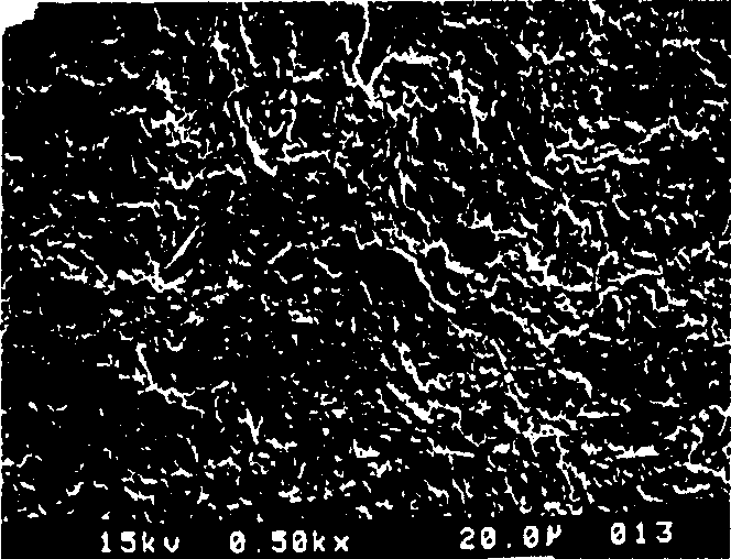
[0123] In addition, the surface conditions observed with a 500-magnification scanning electron microscope (SEM) are as follows: figure 2 shown. There are less than 10 grinding traces in the range of about 240 μm perpendicular to the processing traces on the target. However, unlike the polishing traces of the comparative examples described later, they were not clearly observed, and the roundness was slightly lowered.
Embodiment 3
[0125] Grinding and adjusting the thickness with No. 170 grindstone on the flat grinding disc as in Example 1, and then grinding three times with No. 400, No. 600 and No. 1000. Then, surface treatment was performed with YAG:Nd laser (wavelength: 1064 nm).
[0126] The irradiation conditions of YAG laser are: spot size φ2mm, pulse width 10ns, peak energy 320MW / cm 2 , The pulse frequency is 10Hz, and the average output of one pulse is 100mJ / pulse. The average effective irradiation energy is 3.2J / cm 2 .
[0127] The surface roughness Ra after the surface treatment was measured in accordance with JIS B0601 and found to be 0.50 μm.
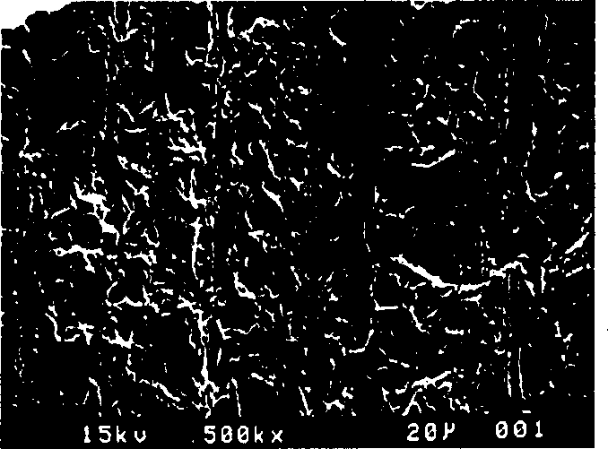
[0128] In addition, the surface conditions observed with a 500-magnification scanning electron microscope (SEM) are as follows: image 3 shown. No linear grinding marks were observed in the range of about 175 μm × 240 μm on the target.
PUM
| Property | Measurement | Unit |
|---|---|---|
| Surface roughness | aaaaa | aaaaa |
| Surface roughness | aaaaa | aaaaa |
| Surface roughness | aaaaa | aaaaa |
Abstract
Description
Claims
Application Information