

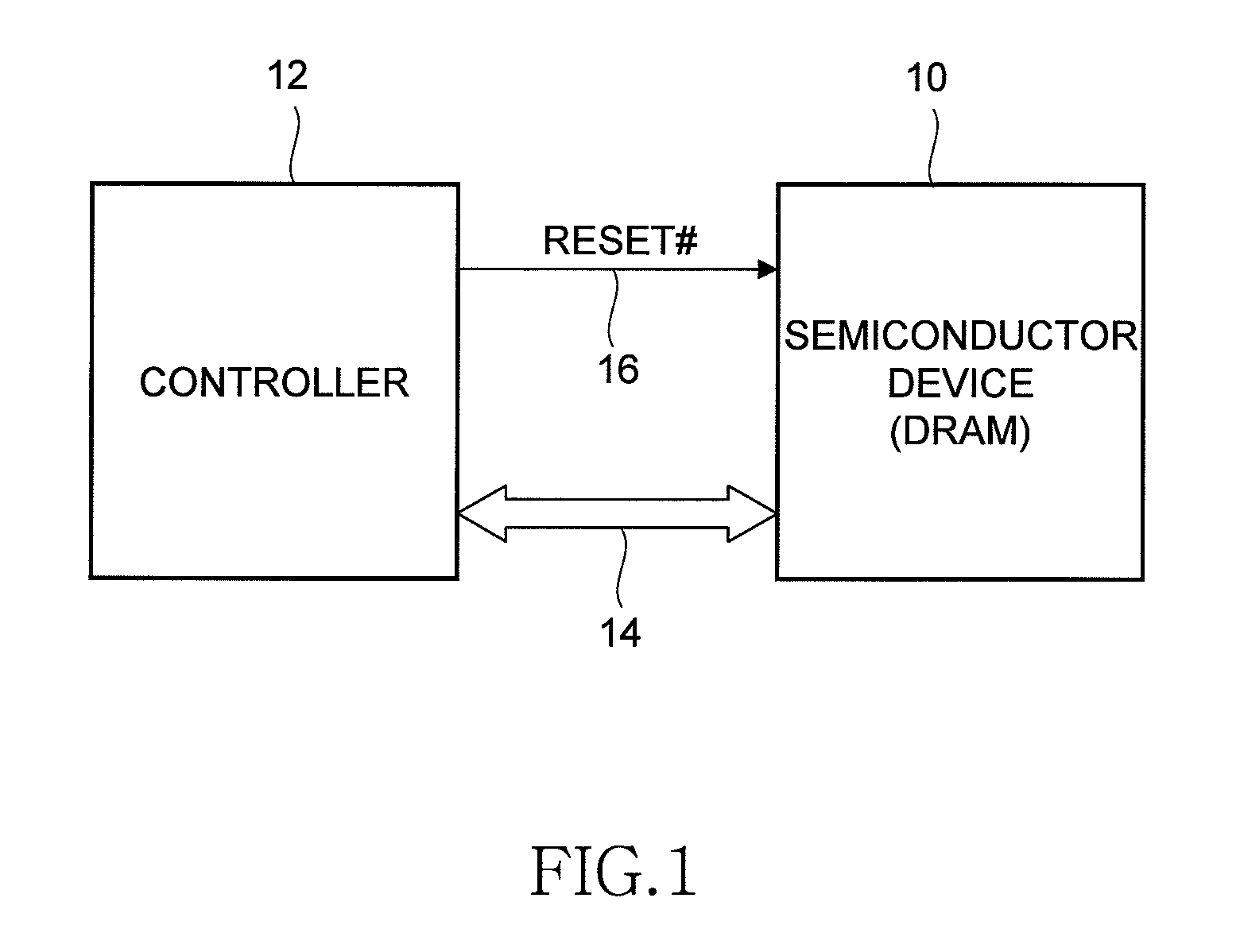
Semiconductor device having nonvolatile memory element and data processing system including the same
a nonvolatile memory element, data processing system technology, applied in static storage, digital storage, instruments, etc., can solve the problems of negligible current flowing through the nonvolatile memory element, the period during which the output of the latch circuit is unstable becomes minimized, and the current consumption at the time of reset can be reduced.
- Summary
- Abstract
- Description
- Claims
- Application Information
AI Technical Summary
Benefits of technology
Problems solved by technology
Method used
Image

Examples
first embodiment
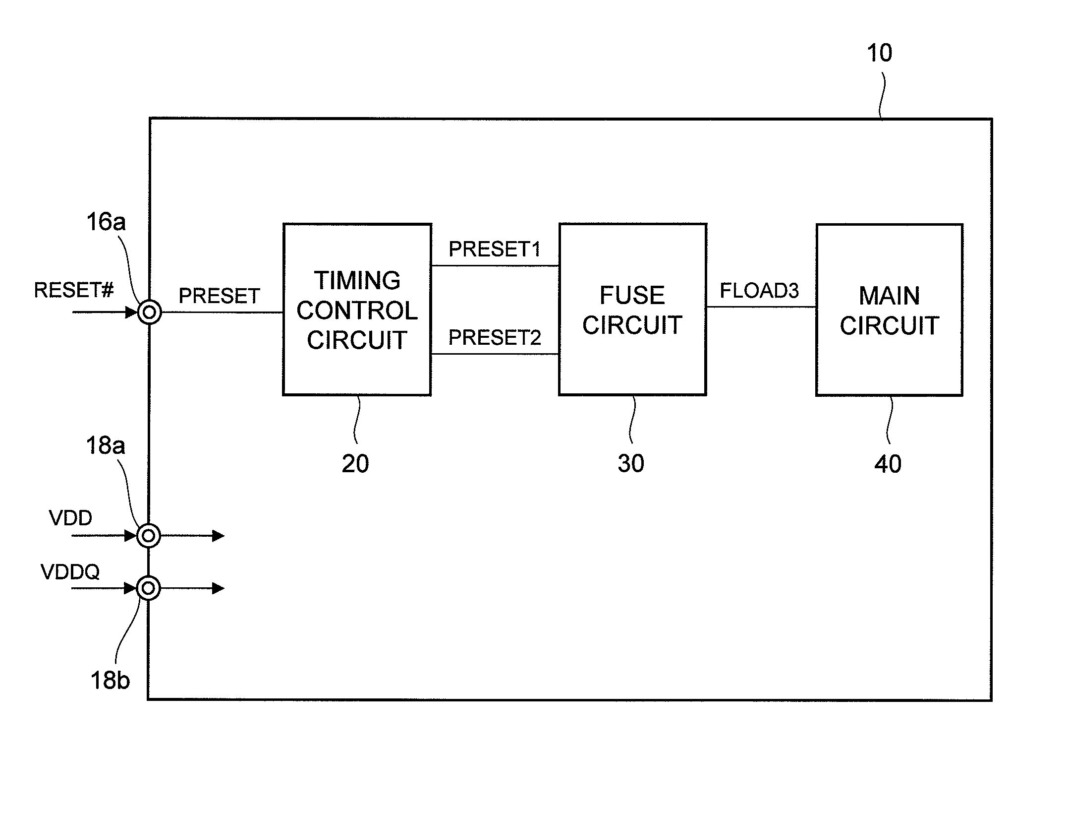
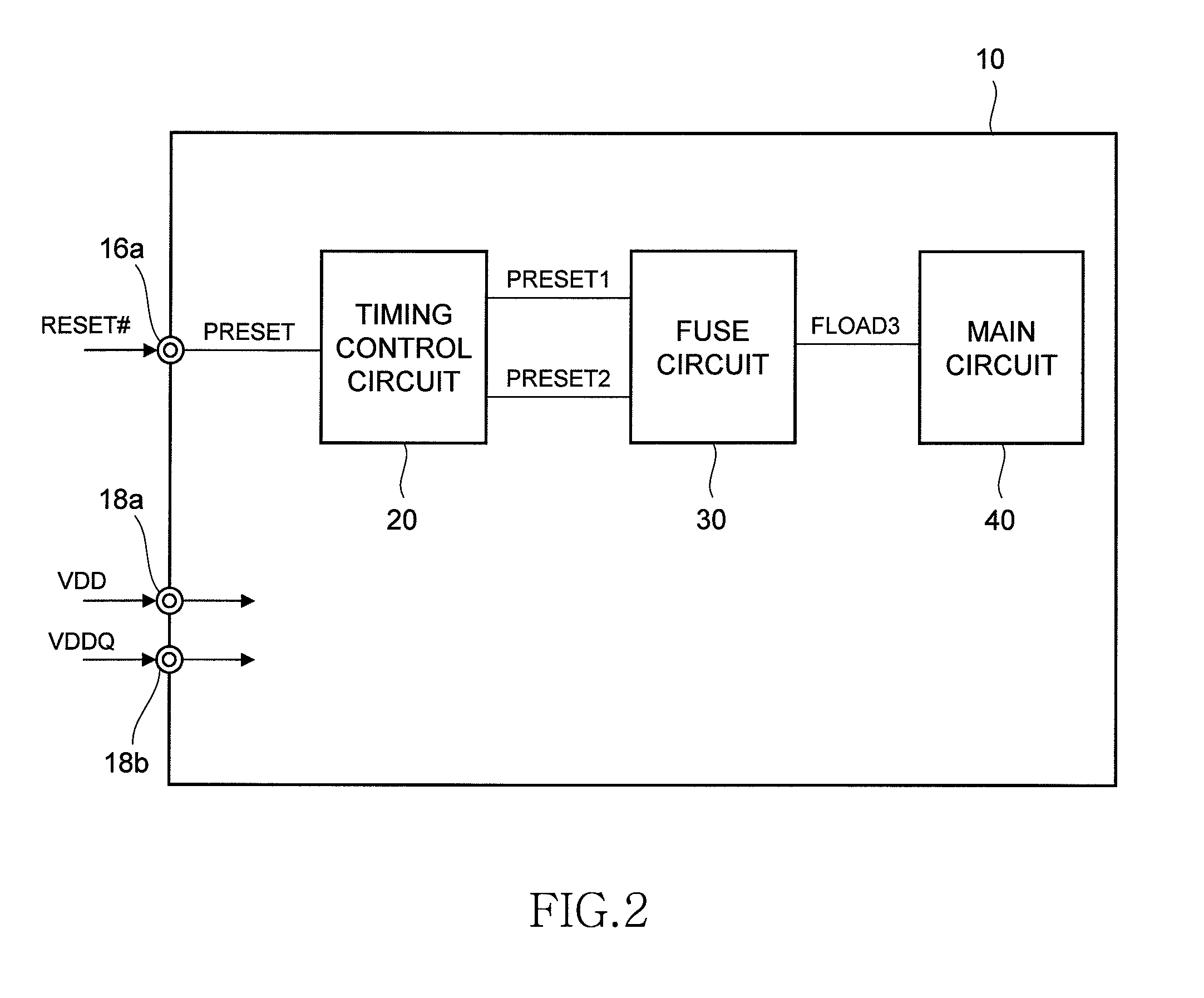
[0052]FIG. 2 is a block diagram of the semiconductor device 10 according to the present invention.
[0053]As shown in FIG. 2, the semiconductor device 10 according to the first embodiment includes a timing control circuit 20, a fuse circuit 30, and a main circuit 40. The main circuit 40 is a circuit block for realizing main functions of the semiconductor device 10, and when the semiconductor device 10 is a DRAM as is the case of the first embodiment, the main circuit 40 is corresponding to a memory core and its peripheral circuits. The peripheral circuits indicate circuit blocks including an address buffer, an address decoder, a command decoder, a refresh counter, a clock control circuit, and a data input / output circuit.
[0054]The timing control circuit 20 is connected to a reset terminal 16a to which the external reset signal RESET# is input. The timing control circuit 20 generates internal reset signals PRESET1 and PRESET2 based on an internal reset signal PRESET that is an internal ...
second embodiment
[0086]the present invention is explained next.
[0087]FIG. 10 is a block diagram of a semiconductor device 10a according to the second embodiment.
[0088]As shown in FIG. 10, the second embodiment is different from the first embodiment in that the semiconductor device 10a further includes a power-on reset-signal generating circuit 50 and the timing control circuit 20 is replaced with a timing control circuit 20a. Because other features of the semiconductor device 10a are the same as those of the semiconductor device 10, like reference numerals are denoted to like constituent elements and redundant explanations thereof will be omitted.
[0089]The power-on reset-signal generating circuit 50 is connected to the power source terminals 18a and 18b, and detects the power source voltages VDD and VDD1 that are supplied to the power source terminals 18a and 18b. A power-on reset signal PON, which is the output of the power-on reset-signal generating circuit 50, is set to the High level (virtually ...
third embodiment
[0095]A semiconductor device according to the present invention is explained next.
[0096]The third embodiment is different from the second embodiment in that the timing control circuit 20a is replaced with a timing control circuit 20b. Therefore, a block diagram showing the entire configuration of the semiconductor device according to the third embodiment will be omitted.
[0097]FIG. 13 is a circuit diagram of the timing control circuit 20b that is employed in the semiconductor device according to the third embodiment.
[0098]As shown in FIG. 13, in the timing control circuit 20b, the AND circuit 25 shown in FIG. 11 is replaced with a NOR circuit 27. Other features of the timing control circuit 20b are the same as those of the timing control circuit 20a shown in FIG. 11.
[0099]FIG. 14 is a timing chart for explaining an operation of the semiconductor device according to the third embodiment.
[0100]As shown in FIG. 14, in the third embodiment, the internal reset signal PRESET1 is activated ...
PUM
 Abstract
Description
Claims
Application Information