Planarized sacrificial layer for MEMS fabrication

a technology of microelectromechanical and sacrificial layer, which is applied in the direction of piezoelectric/electrostrictive transducers, generators/motors, transducer types, etc., can solve the problems of reducing the performance and stability of the mems device, the release area formed where the sacrificial material was removed is too large, and the anchoring of the component is not controlled in a controlled manner, so as to facilitate easy control of the thickness of the component a mems device and a mems device and a planarized sacrificial layer and mems device and a mems device and a technology of mems device and a technology of mems device and a technology of a mems device and a technology of a mems device and a technology of a semiconductor device and a technology of a semiconductor applied in the field of mems device and a semiconductor device thickness thickness, a technology applied in the field a technology of mems device and a technology of a mems device and a technology of a mems device and a technology of a m

Active Publication Date: 2012-10-02
QORVO US INC
View PDF11 Cites 100 Cited by
  • Summary
  • Abstract
  • Description
  • Claims
  • Application Information

AI Technical Summary

Benefits of technology

[0006]According to the present invention, a component is formed, where a cavity is formed below the component in order to allow movement of the component. Initially, a sacrificial layer and a field layer are deposited and patterned on a substrate and then planarized. The component, which may be a Microelectromechanical Systems (MEMS) resonator, is formed over the planarized sacrificial layer. Moreover, anchors of the component are formed substantially over the field layer. The sacrificial layer is then removed such that the field layer remains on the substrate around the area from which the sacrificial layer is removed. When the sacrificial layer is removed, the cavity is formed below the component, which allows movement of the component during operation. The field layer is formed on the substrate such that a substantial portion of the component anchors are formed over the field layer. Thus, when the sacrificial layer is removed, the component anchors remain anchored over the field such that the component anchors are not substantially disposed over the cavity, thereby improving anchoring of the component along with device performance and device stability.
[0007]Since the sacrificial layer is planarized, components formed on the sacrificial layer may easily integrate with different types of circuitries, such as CMOS circuitries. Specifically, the planar topography of the sacrificial layer minimizes the difficulties associated with patterning electrodes and other MEMS structures on the sacrificial layer. Furthermore, planarization of the sacrificial layer facilitates easily controlling the thickness of the component.
[0008]In accordance with an embodiment of the present invention, the sacrificial layers used to form the cavity in the MEMS device are formed with a material selected for its etching capabilities, such that during etching of the sacrificial layer, etching of other structures, such as the substrate, the field layer, and the component, is minimized.

Problems solved by technology

However, the sacrificial material is not removed in a controlled manner beneath the MEMS device.
Thus, a release area formed where the sacrificial material was removed becomes too large.
However, when the sacrificial material disposed under the anchors is removed, performance and stability of the MEMS device degrades, thereby degrading overall performance and reliability of the MEMS device.
However, the piezoelectric substrate may warp at the region where the cavity is formed prior to thinning down.
Furthermore, thinning down the piezoelectric substrate increases warping.
Thus, performance of a device employing the warped piezoelectric substrate dramatically degrades, thereby making a device manufactured according to this method undesirable.

Method used


Image

  • Planarized sacrificial layer for MEMS fabrication
  • Planarized sacrificial layer for MEMS fabrication
  • Planarized sacrificial layer for MEMS fabrication

Examples


Embodiment Construction

[0024]The embodiments set forth below represent the necessary information to enable those skilled in the art to practice the invention and illustrate the best mode of practicing the invention. Upon reading the following description in light of the accompanying drawing figures, those skilled in the art will understand the concepts of the invention and will recognize applications of these concepts not particularly addressed herein. It should be understood that these concepts and applications fall within the scope of the disclosure and the accompanying claims.

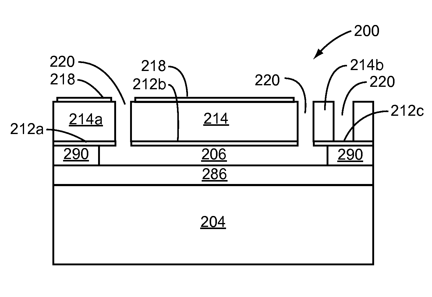
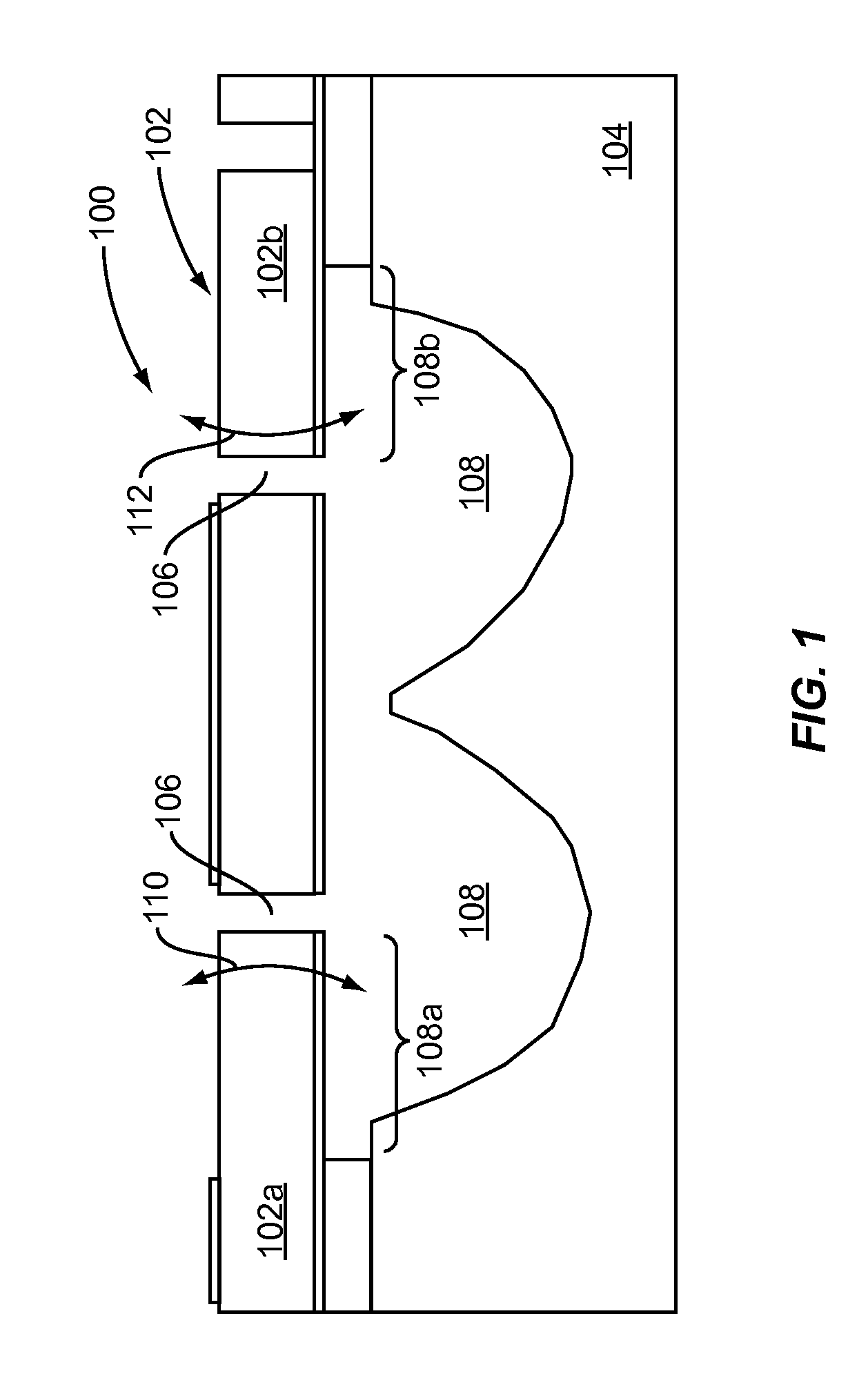
[0025]According to the present invention, a component is formed, where a cavity is formed below the component in order to allow movement of the component. Initially, a sacrificial layer and an field layer are deposited and patterned on a substrate and then planarized. The component, which may be a Microelectromechanical Systems (MEMS) resonator, is formed over the planarized sacrificial layer. Moreover, anchors of the component ar...


PUM

PropertyMeasurementUnit
thicknessaaaaaaaaaa
thicknessaaaaaaaaaa
thicknessaaaaaaaaaa

Abstract

A method of forming a device is provided. The method includes providing a substrate, forming a sacrificial layer over the substrate, and forming an field layer around the sacrificial layer. After formation, both the sacrificial layer and the field layer are planarized. A component is then formed over the planarized sacrificial layer and the planarized field layer. The component has a first electrode and a second electrode and a single crystal wafer disposed between the first electrode and the second electrode. The component also includes anchors disposed substantially over the field layer. Once the component is formed, the sacrificial layer is released with an etchant having a selectivity for the sacrificial layer such that a cavity is formed beneath the component. The cavity allows free movement component within the cavity during operation of the device. In addition, the etchant does not release the field layer and the component such that the field layer remains below the anchors.

Description

RELATED APPLICATION[0001]This application claims the benefit of Provisional Patent Application Ser. No. 61 / 047,477, filed Apr. 24, 2008, the disclosure of which is hereby incorporated by reference in its entirety.FIELD OF THE INVENTION[0002]The present invention generally relates to Microelectromechanical (MEMS) devices and more particularly to forming a package for a semiconductor device or a MEMS device.BACKGROUND OF THE INVENTION[0003]Various types of micromechanical components operate best in an open area cavity. In particular, portions of MEMS devices, such as portions of MEMS resonators should be suspended in air within a device to maximize energy reflection between the MEMS resonator and air. In order to suspend a portion of a MEMS device in air, during fabrication, MEMS devices are formed over a sacrificial material, which is subsequently removed, thereby providing the MEMS device portion with free space and allowing movement. However, the sacrificial material is not removed...

Claims


Application Information

Patent Timeline
Patent Type & Authority Patents(United States)
IPC IPC(8): H01L21/00
CPCH01L21/00Y10T29/42B81C1/00476
Inventor LEE, SEUNGBAELI, SHENG-SHIANBHATTACHARJEE, KUSHAL
Owner QORVO US INC
Why Eureka
Try Eureka