Flexible light-emitting device, and method for fabricating the same

a light-emitting device and flexible technology, applied in non-linear optics, instruments, transportation and packaging, etc., can solve the problems of low heat resistance and difficulty in forming a tft using a crystalline semiconductor with high mobility, and achieve high-quality images and high-quality images

Active Publication Date: 2012-10-09
SEMICON ENERGY LAB CO LTD
View PDF138 Cites 115 Cited by
  • Summary
  • Abstract
  • Description
  • Claims
  • Application Information

AI Technical Summary

Benefits of technology

[0010]According to one embodiment of the present invention, it is an object to provide a flexible light-emitting device provided with a TFT using a crystalline semiconductor which enables displaying of a high-quality image.
[0015]One embodiment of the present invention is a flexible light-emitting device provided with a TFT using a crystalline semiconductor which enables displaying of a high-quality image.
[0016]Another embodiment of the present invention is a method for manufacturing a flexible light-emitting device provided with a TFT using a crystalline semiconductor which enables displaying of a high-quality image.

Problems solved by technology

Therefore, it has been difficult to form a TFT using a crystalline semiconductor with high mobility over a flexible substrate with low heat resistance.

Method used


Image

  • Flexible light-emitting device, and method for fabricating the same
  • Flexible light-emitting device, and method for fabricating the same
  • Flexible light-emitting device, and method for fabricating the same

Examples


embodiment 1

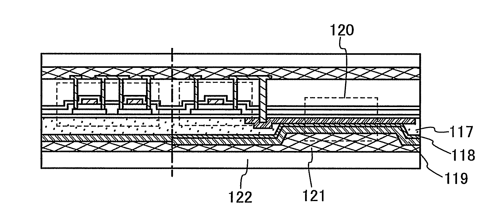
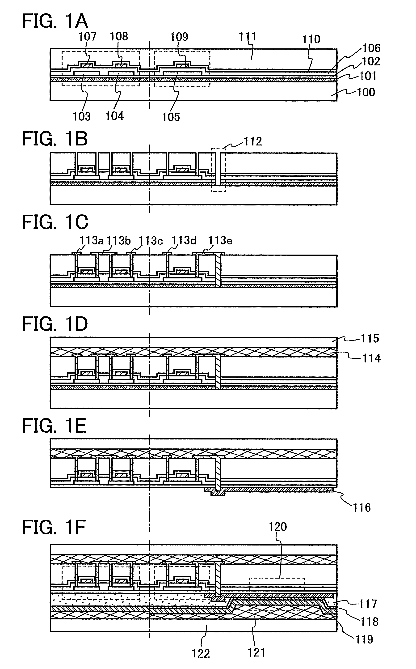
[0024]FIGS. 1A to 1F show an example of a method for manufacturing a flexible light-emitting device of one embodiment of the present invention. A separation layer 101, a base insulating film 102, crystalline semiconductor layers 103, 104, and 105, a gate insulating film 106, gate electrodes 107, 108, and 109, a passivation film 110, and an interlayer insulating film 111 are formed over a formation substrate 100 (see FIG. 1A). Note that the passivation film 110 may be omitted. As the formation substrate 100, a substrate such as a glass substrate or a ceramics substrate, which can withstand heat applied at the time of formation of the crystalline semiconductor layers 103 to 105, is used. In the present specification, as the crystalline semiconductor layers 103 to 105, a polycrystalline semiconductor or a microcrystalline semiconductor is used which needs to be subjected to crystallization and improvement in crystallinity at a temperature of at least 400° C. Further, a single crystal s...

embodiment 2

[0117]FIGS. 5A to 5C are a top view and cross-sectional views of light-emitting devices of module type (also referred to as EL modules).

[0118]FIG. 5A is a top view for showing an EL module, and FIG. 5B is a drawing showing part of a cross section taken along line A-A′ of FIG. 5A. In FIG. 5A, reference numeral 500 denotes a flexible printed circuit (FPC) that is an external input terminal; reference numeral 508 denotes a wiring for transmitting a signal to be input to a source side driver circuit 504 and a gate side driver circuit 503; and reference numeral 502 denotes a pixel portion. The pixel portion and the driver circuits can be manufactured according to Embodiment 1 described above.

[0119]The FPC 500 is an external input terminal which transmits a video signal or a clock signal to the source side driver circuit 504 and the gate side driver circuit 503. Note that only the FPC 500 is shown here; however, a printed wiring board (PWB) may be attached to the FPC. The light emitting d...

embodiment 3

[0124]In this embodiment, electronic devices each including the light-emitting device described in Embodiment 1 or Embodiment 2 will be described.

[0125]Examples of the electronic devices each including the light-emitting device described in Embodiment 1 or Embodiment 2 include cameras such as video cameras or digital cameras, goggle type displays, navigation systems, audio playback devices (e.g., car audio systems and audio systems), computers, game machines, portable information terminals (e.g., mobile computers, cellular phones, portable game machines, and electronic books), image playback devices in which a recording medium is provided (specifically, devices that are capable of playing back recording media such as digital versatile discs (DVDs) and equipped with a display unit that can display images), and the like. Specific examples of these electronic devices are shown in FIGS. 6A to 6E.

[0126]FIG. 6A shows a television device which includes a housing 9101, a supporting base 910...


PUM

PropertyMeasurementUnit
temperatureaaaaaaaaaa
frequencyaaaaaaaaaa
temperaturesaaaaaaaaaa

Abstract

Provided is a flexible light-emitting device including: a base insulating film; a thin film transistor formed over a first surface of the base insulating film; an interlayer insulating film formed over the first surface of the base insulating film with the thin film transistor interposed therebetween; a first pixel electrode formed on a second surface of the base insulating film opposite to the first surface; an electroluminescent layer formed on the second surface of the base insulating film with the first pixel electrode interposed therebetween; a second pixel electrode formed on the second surface of the base insulating film with the first pixel electrode and the electroluminescent layer interposed therebetween; and a wiring electrically connected to a semiconductor layer of the thin film transistor in a contact hole provided in the interlayer insulating film and electrically connected to the first pixel electrode in a through-hole penetrating through at least the interlayer insulating film and the base insulating film.

Description

BACKGROUND OF THE INVENTION[0001]1. Field of the Invention[0002]The present invention relates to a light-emitting device which has a circuit including a thin film transistor (hereinafter also referred to as a TFT) using a crystalline semiconductor layer and fabricating the light-emitting device. In addition, the present invention relates to an electronic device mounted with such a light-emitting device.[0003]2. Description of the Related Art[0004]In recent years, a technological development has been remarkably made in the field of displays. In particular, the needs of the market have stimulated tremendous progress in the technology directed to increase in resolution of displays and thinning of displays.[0005]In a next phase of this field, focus is placed on commercialization of a flexible display having a curved display area. Further, a light-emitting device using a flexible substrate can be made lightweight as compared to the case of using a glass substrate or the like. A variety o...

Claims


Application Information

Patent Timeline
Patent Type & Authority Patents(United States)
IPC IPC(8): G02F1/1345B60Q1/14H01L21/00
CPCH01L27/1225H01L27/1266H01L27/3244H01L27/3248H01L27/1248H01L51/56H01L27/124H01L2227/326H01L2251/5338H01L27/3276H10K59/123H10K59/12H10K59/131H10K71/80H10K59/1201H10K2102/311H10K71/00H01L27/1214H01L27/1218
Inventor CHIDA, AKIHIROHATANO, KAORUNAGATA, TAKAAKISEO, SATOSHI
Owner SEMICON ENERGY LAB CO LTD
Why Eureka
Try Eureka