Method and system for hybrid integrated 1XN DWDM transmitter

a transmitter and hybrid technology, applied in multiplex communication, instruments, optical elements, etc., can solve the problems of reducing the effectiveness of broader applications, limiting the use of broader applications, and moving toward the packaging cost of each individual optical component, so as to reduce the cost and system footprint, increase product reliability and manufacture yield, and good thermal conductivity of aln

Active Publication Date: 2012-10-09
FUTUREWEI TECH INC
View PDF113 Cites 8 Cited by
  • Summary
  • Abstract
  • Description
  • Claims
  • Application Information

AI Technical Summary

Benefits of technology

[0013]Many benefits are achieved by way of the present invention over conventional techniques. For example, in certain embodiments, the invention provides a method of integrating various optical components using excellent CTE match between InP and AlN as well as good thermal conductivity of AlN. According to embodiments of the present invention, the method is readily scaleable to large laser array chips for further reduction of cost and system footprint as well as increasing product reliability and manufacture yield. According to certain embodiments of the invention, large array chips can enable further improvements of optical coupling between AWG and transmitters. For example, vertical variation in height relative to the waveguides can be minimized from transmitter to transmitter if these transmitters are formed on a single array chip. In contrast, large array chips can not be used in conventional flip-chip bonding due to CTE mismatch and, therefore, the vertical height varies from chip to chip, giving rise to non-uniform coupling efficiencies.
[0014]Some embodiments of the present invention provides techniques that reduce the complexities in product manufacturing in that quality control can be easily carried out at different levels of the integration. For example, the laser array on AlN may be manufactured by a specialist, and the final integration can be reduced to a simple alignment of the array with AWG and can be manufactured by using conventional packaging houses in the industry. Therefore, performance deviation of the final product is minimal and its packaging yield may be substantially higher than integrating InP chips directly on PLC. In specific embodiments, techniques are provided for using a butt joint method for optical coupling between laser array and AWG. As a result, the coupling efficiency is expected to be high. In an embodiment, both laser / waveguide surfaces can be AR coated to reduce reflection loss as well as possible back reflection into the laser cavity for high laser performance and stability. In some embodiments, the invention provides a method and system for using micro heaters to adjust a center frequency of each individual laser in the transmitter.

Problems solved by technology

Now the price bottleneck is moving toward the packaging cost of each individual optical component, such as lasers, modulators, and MUX / DEMUX filters.
The packaging cost of these components (e.g., a 10 G transmitter) becomes a bottleneck, preventing further reduction in price.
Even though these conventional DWDM systems are useful in some areas, they have many limitations that restrict their effectiveness in broader applications.

Method used


Image

  • Method and system for hybrid integrated 1XN DWDM transmitter
  • Method and system for hybrid integrated 1XN DWDM transmitter
  • Method and system for hybrid integrated 1XN DWDM transmitter

Examples


Embodiment Construction

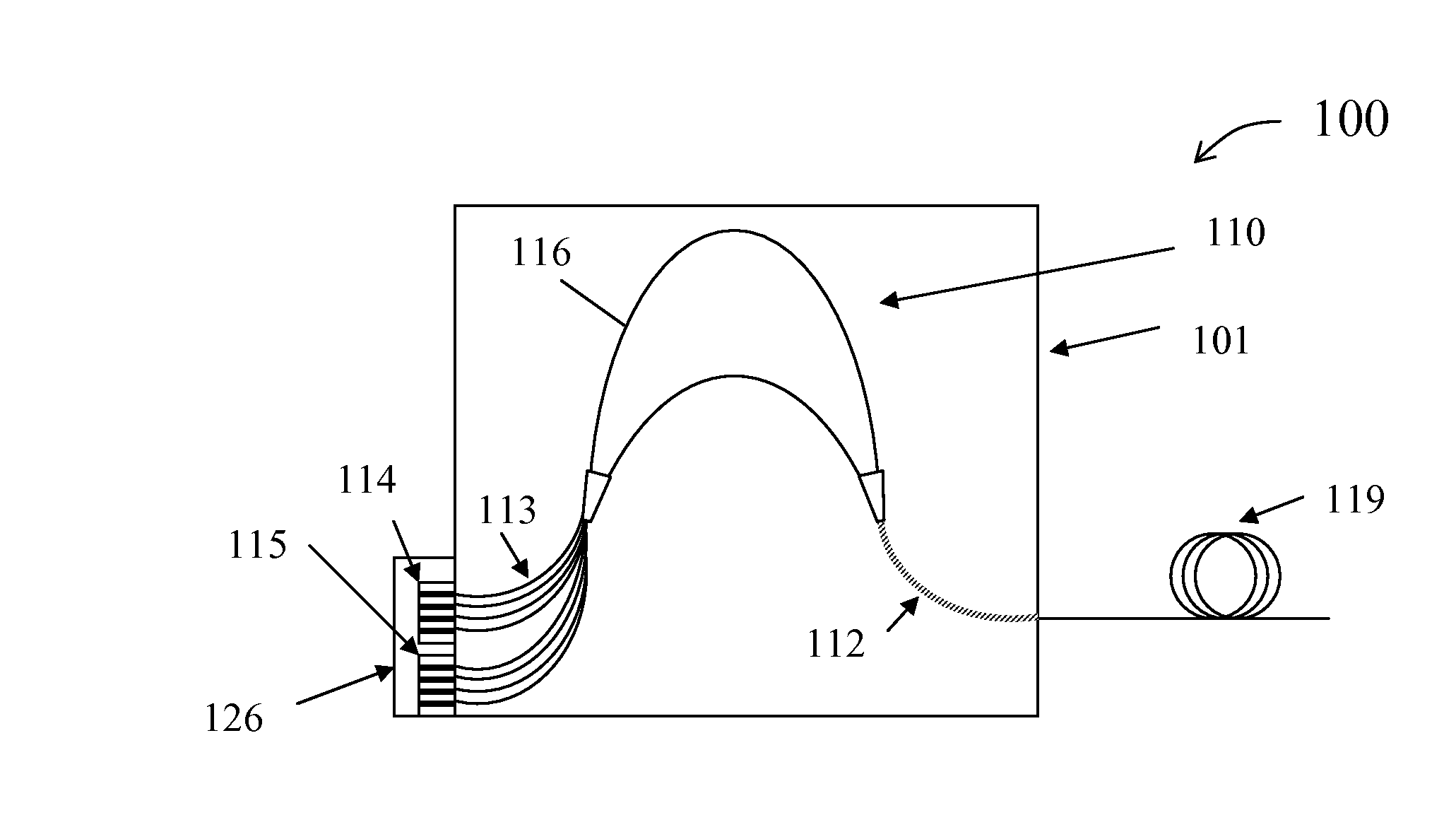
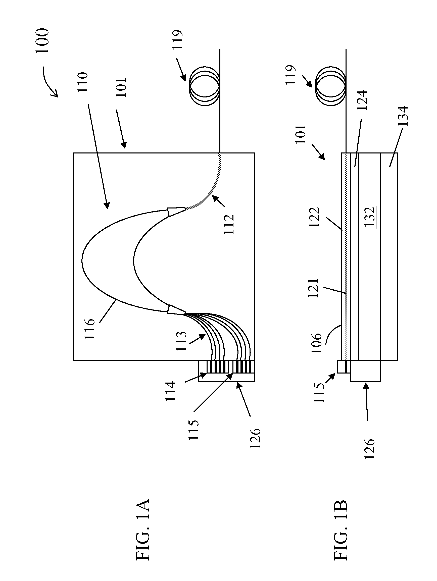
[0026]The present invention is directed to fiber optical transport systems. More particularly, the invention provides a method and system for integrating semiconductor (InP) laser / modulator chips on an aluminum nitride submount with a silica / silicon AWG. Merely by way of example, the invention has been applied to a wavelength multiplexed transmitter array. But it would be recognized that the invention has a much broader range of applicability.

[0027]As discussed above, the optical components in a conventional DWDM system are usually individually packaged. Discrete optical components often have large footprint and hence bulky in size. For example, a 10 G transmitter in a Butterfly package has typical dimensions of approximately 30×14×11.5 mm. If the line side of a DWDM system requires 12 such transmitters, it occupies a sizable space too large to fit onto a conventional line card. Multiple line cards and hence shelves are needed to support high DWDM channel counts, giving rise to a bo...


PUM


Abstract

An integrated DWDM transmitter apparatus includes a silica-on-silicon substrate overlying a first support component. The silica-on-silicon substrate includes a silica layer overlying a silicon layer. A coefficient of thermal expansion of the first support component is substantially matched to a coefficient of thermal expansion of the silicon layer. An optical multiplexer is located within the silica layer and includes a plurality of input waveguides and at least an output waveguide. Additionally, the apparatus includes a second support component attached to a side surface of the first support component. One or more semiconductor laser array chips overlie the second support component. A coefficient of thermal expansion of the one or more semiconductor chips is substantially matched to a coefficient of thermal expansion of the second support component. Moreover, each of the one or more laser array chips includes one or more lasers, each of which is optically coupled to a corresponding one of the plurality of input waveguides.

Description

CROSS-REFERENCES TO RELATED APPLICATIONS[0001]This application claims priority to U.S. Provisional Patent Application No. 60 / 862,391, filed Oct. 20, 2006, commonly assigned, incorporated herein by reference for all purposes.[0002]Additionally, this application is related to co-pending U.S. patent application Ser. No. 11 / 844,969, filed Aug. 24, 2007, which is a continuation-in-part of U.S. patent application Ser. No. 11 / 696,472, filed Apr. 4, 2007, which claims priority to U.S. Provisional Patent Application No. 60 / 827,825, filed Oct. 2, 2006, all commonly assigned. The entire content of U.S. patent application Ser. No. 11 / 696,472 and U.S. patent application Ser. No. 11 / 844,969 are hereby incorporated by reference for all purposes.BACKGROUND OF THE INVENTION[0003]The present invention is directed to fiber optical transport systems. More particularly, the invention provides a method and system for integrating semiconductor (InP) laser / modulator chips on an aluminum nitride submount wi...

Claims


Application Information

Patent Timeline
Patent Type & Authority Patents(United States)
IPC IPC(8): H04B10/04G02B6/12
CPCG02B6/12019G02B6/1203H04J14/02
Inventor SHEN, XIAO ANDYBAI, YU SHENG
Owner FUTUREWEI TECH INC
Why Eureka
Try Eureka