Polarized white light devices using non-polar or semipolar gallium containing materials and transparent phosphors

a technology of non-polar or semi-polar gallium and white light, applied in the field of lighting techniques, can solve the problems of low efficiency, low efficiency, and low efficiency of conventional edison light bulbs, and achieve the effect of improving efficiency and being easy to implemen

Active Publication Date: 2012-10-30
SLT TECH
View PDF143 Cites 67 Cited by
  • Summary
  • Abstract
  • Description
  • Claims
  • Application Information

AI Technical Summary

Benefits of technology

[0014]One or more benefits may be achieved using one or more of the specific embodiments. As an example, the present device and method provides for an improved lighting technique with improved efficiencies. In other embodiments, the present method and resulting structure are easier to implement using conventional technologies. In some embodiments, the present device and method provide polarized light at two or more wavelengths that are useful in displays and in conjunction with polarizing transmission filters. In a specific embodiment, the blue LED device is capable of emitting electromagnetic radiation at a wavelength range from about 450...

Problems solved by technology

Unfortunately, drawbacks exist with the conventional Edison light bulb.
Additionally, the conventional light bulb routinely fails, often due to thermal expansion and contraction, of the filament element.
Unfortunately, achieving high intensity, high-efficiency GaN-based green LEDs has been particularly problematic.
The performance of optoelectronic devices fabricated on conventional c-plane GaN suffer from strong internal polarization fields, which spatially separate the electron and hole wave functions and lead to poor radiative recombination efficiency.
Since this phenomenon becomes more pronounced in InGaN layers with increased indium content for increased wavelength emission, extending the performance of UV or blue GaN-based LEDs to the blue-green or green regime has been difficult.
Furthermore, since increased indium content films often require reduced growth temperature, the crystal quality of the InGaN films is ...

Method used


Image

  • Polarized white light devices using non-polar or semipolar gallium containing materials and transparent phosphors
  • Polarized white light devices using non-polar or semipolar gallium containing materials and transparent phosphors
  • Polarized white light devices using non-polar or semipolar gallium containing materials and transparent phosphors

Examples


example 1

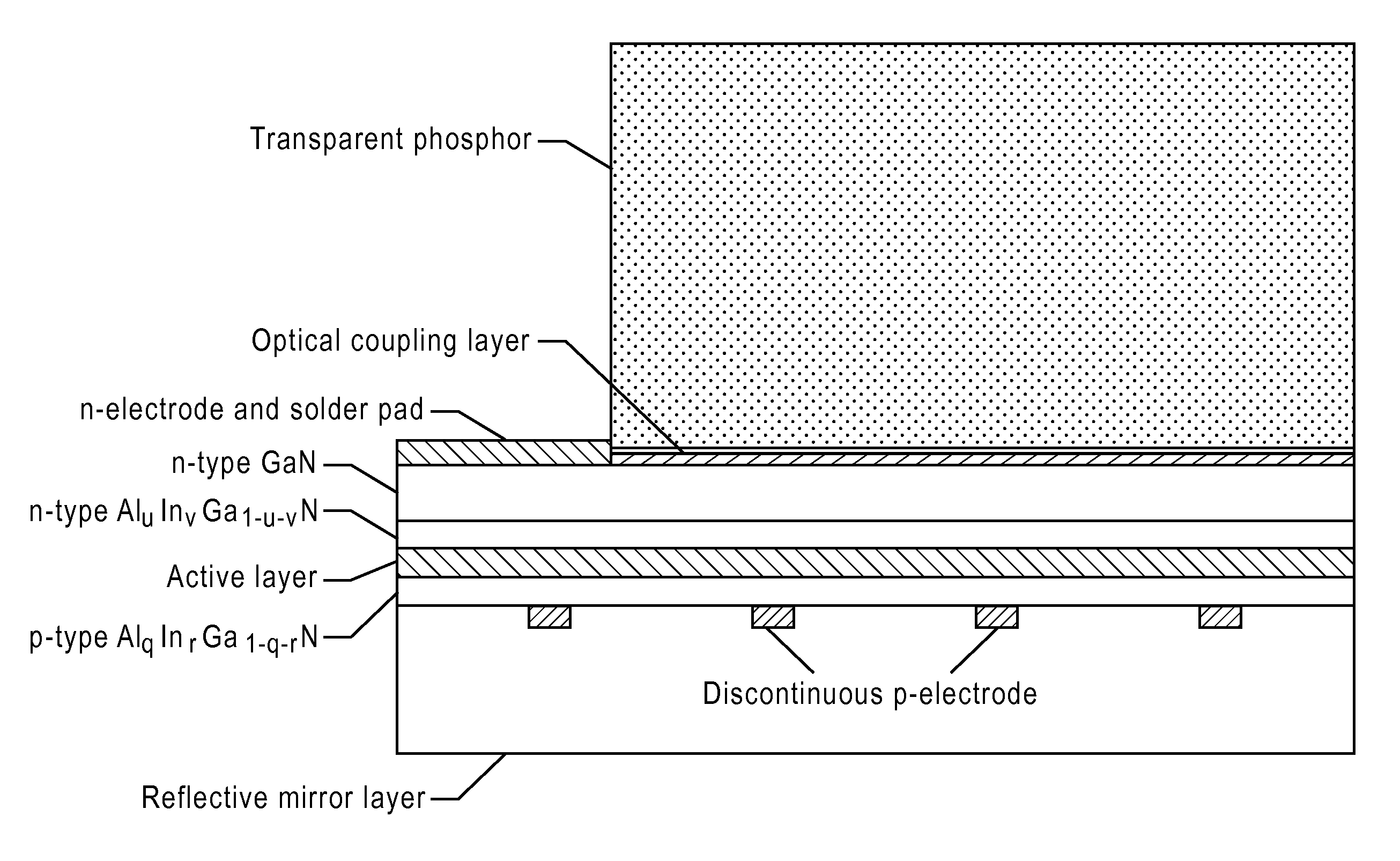
[0121]To prove the operation and method of the present invention, we performed experiments and provide these examples. These examples are illustrative and should not limit the scope of the claims herein. One of ordinary skill in the art would recognize other variations, modifications, and alternatives. In our example, metallic p-type contacts (Ni / Au / Ti / Au) were formed overlying the p-GaN contact layer of an LED device structure emitting electromagnetic radiation at a nominal wavelength of 450 nm, provided on a bulk non-polar GaN substrate. The LED device structure was generally conventional in design, although other device structures can be used according to other embodiments and / or examples. Next, 300 um×300 um LED mesas were then defined using a Cl2 based reactive ion etch. The backside of the substrate was then polished using a chemical-mechanical polishing process, resulting in an optically flat and transparent back surface. Metallic indium was then deposited in contact with the...


PUM


Abstract

A light emitting device includes a substrate having a surface region and a light emitting diode overlying the surface region. The light emitting diode is fabricated on a semipolar or nonpolar GaN containing substrate and emits electromagnetic radiation of a first wavelength. The diode includes a quantum well region characterized by an electron wave function and a hole wave function. The electron wave function and the hole wave function are substantially overlapped within a predetermined spatial region of the quantum well region. The device has a transparent phosphor overlying the light emitting diode. The phosphor is excited by the substantially polarized emission to emit electromagnetic radiation of a second wavelength.

Description

CROSS-REFERENCES TO RELATED APPLICATIONS[0001]This application claims priority to U.S. Provisional Application No. 61 / 167,447 filed Apr. 7, 2009, commonly assigned, and hereby incorporated by reference.BACKGROUND OF THE INVENTION[0002]This invention relates generally to lighting techniques. More specifically, embodiments of the invention include techniques for combining one or more colored light emitting diodes (LEDs), such as violet, blue, blue and yellow, or blue and green, fabricated on bulk semipolar or nonpolar materials with use of materials such as phosphors, which emit light. In other embodiments, the entities may be also any wavelength conversion material(s) or energy conversion material(s), or the like. Herein the term “phosphor” is used to include all such types of materials. Merely by way of example, the invention can be applied to applications such as white lighting, multi-colored lighting, general illumination, decorative lighting, automotive and aircraft lamps, street...

Claims


Application Information

Patent Timeline
IPC IPC(8): H01L27/15H01L33/00
CPCH01L33/44H01L33/507H01L33/32H01L33/50H01L33/38H01L33/405H01L33/505H01L2224/48247H01L33/16H01L2224/48091H01L2924/00014H01L2924/12044H01L2924/00
Inventor D'EVELYN, MARK P.SHARMA, RAJATHALL, ERIC M.FEEZELL, DANIEL F.
Owner SLT TECH
Why Eureka
Try Eureka