
Method and system for metal barrier and seed integration

a technology of metal barrier and seed, applied in the field of integrated circuits, can solve the problems of many limitations, large cost of ic fabrication facilities, and difficulty in small devices, and achieve the effects of improving the quality of dielectric and/or metal diffusion layer, preventing metal diffusion, and being convenient to us

Active Publication Date: 2012-11-13
SEMICON MFG INT (SHANGHAI) CORP +1
View PDF7 Cites 0 Cited by
  • Summary
  • Abstract
  • Description
  • Claims
  • Application Information

AI Technical Summary

Benefits of technology

The present invention provides a method for making electrodes in semiconductor devices by integrating dielectric and metal barrier layers. The method includes depositing a dielectric layer and a copper diffusion barrier layer on a substrate, removing the barrier layer from the bottom surface, depositing a seed layer and an electrode layer, and using an AC power level and a DC power level to control the etching and deposition rates. The method can be applied to various semiconductor devices, such as single or dual damascene back-end-of-line (BEOL) integration for making integrated circuits. The technical effects of the invention include improved electrode integration and control over the deposition and etching rates, which enhance the efficiency and reliability of the manufacturing process.

Problems solved by technology

An IC fabrication facility can cost hundreds of millions, or even billions, of dollars.
Making devices smaller is very challenging, as each process used in IC fabrication has a limit.
Although fabless chip companies and foundry services have increased through the years, many limitations still exist.
For example, metal barrier and metal layer may limited reliability.

Method used


Image

  • Method and system for metal barrier and seed integration
  • Method and system for metal barrier and seed integration
  • Method and system for metal barrier and seed integration

Examples


Embodiment Construction

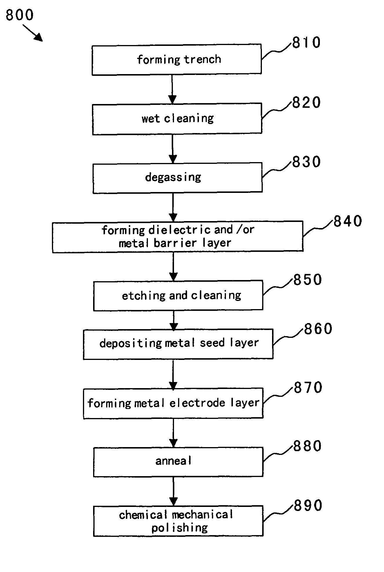
[0033]The present invention is directed to integrated circuits and their processing for the manufacture of semiconductor devices. More particularly, the invention provides a method and device for dielectric and / or metal barrier and seed integration for the manufacture of integrated circuits. Merely by way of example, the invention has been applied to single or dual damascene back-end-of-line (BEOL) integration for the manufacture of integrated circuits. But it would be recognized that the invention has a much broader range of applicability. For example, the invention can be applied to a trench or via for shallow trench isolation or contact formation.

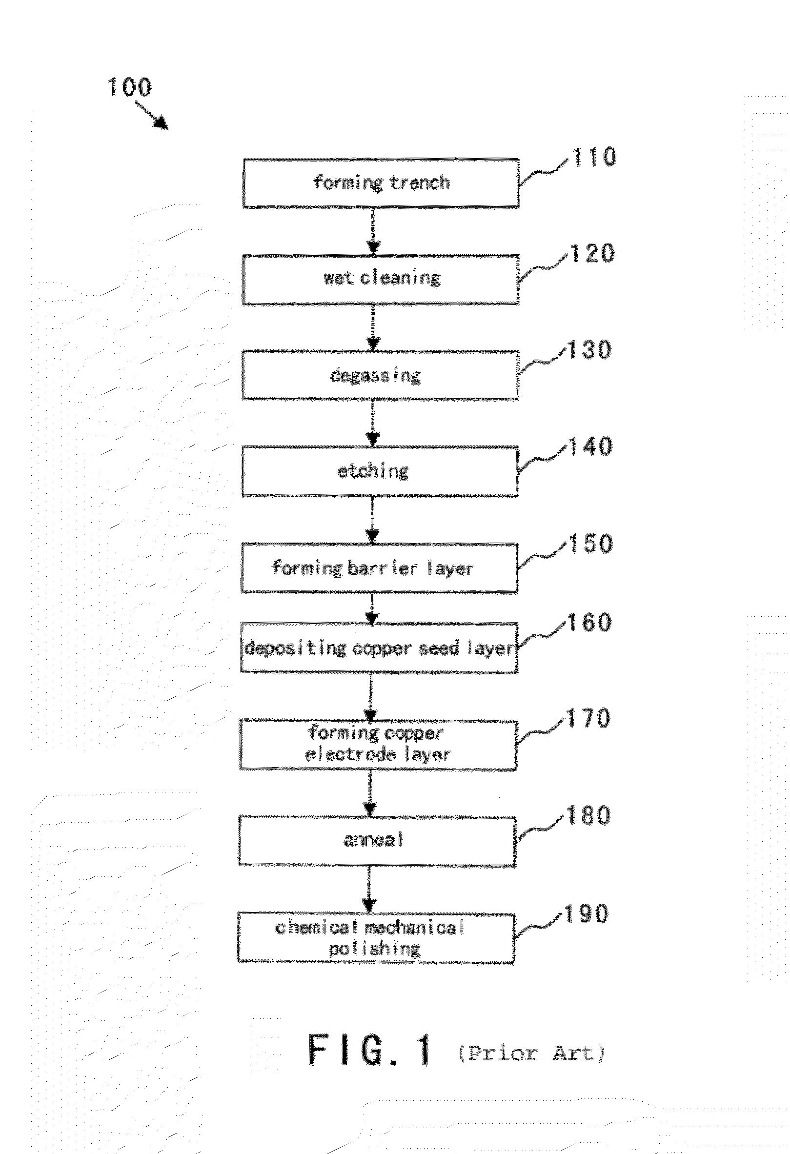
[0034]FIG. 1 is a simplified conventional method for forming metal layer. The method 100 includes the following processes:

[0035]1. Process 110 for forming trench;

[0036]2. Process 120 for wet cleaning;

[0037]3. Process 130 for degassing;

[0038]4. Process 140 for etching;

[0039]5. Process 150 for forming barrier layer;

[0040]6. Process 160 for...


PUM


Abstract

A method for making an electrode in a semiconductor device. The method includes forming a trench in a first layer. The first layer is associated with a top surface, and the trench is associated with a bottom surface and a side surface. Additionally, the method includes depositing a diffusion barrier layer on at least the bottom surface, the side surface, and a part of the top surface, removing the diffusion barrier layer from at least a part of the bottom surface, depositing a seed layer on at least the part of the bottom surface and the diffusion barrier layer, and depositing an electrode layer on the seed layer.

Description

CROSS-REFERENCES TO RELATED APPLICATIONS[0001]This application claims priority to Chinese Patent Application No. 200410084788.5, filed Nov. 24, 2004, commonly assigned, incorporated by reference herein for all purposes.STATEMENT AS TO RIGHTS TO INVENTIONS MADE UNDER FEDERALLY SPONSORED RESEARCH OR DEVELOPMENT[0002]Not ApplicableREFERENCE TO A “SEQUENCE LISTING,” A TABLE, OR A COMPUTER PROGRAM LISTING APPENDIX SUBMITTED ON A COMPACT DISK.[0003]Not ApplicableBACKGROUND OF THE INVENTION[0004]The present invention is directed to integrated circuits and their processing for the manufacture of semiconductor devices. More particularly, the invention provides a method and device for dielectric and / or metal barrier and seed integration for the manufacture of integrated circuits. Merely by way of example, the invention has been applied to single or dual damascene back-end-of-line (BEOL) integration for the manufacture of integrated circuits. But it would be recognized that the invention has a...

Claims


Application Information

Patent Timeline
Patent Type & Authority Patents(United States)
IPC IPC(8): H01L29/04
CPCH01L21/02063H01L21/76802H01L21/76814H01L21/76831H01L21/76843H01L21/76844H01L21/76865H01L21/76871
Inventor ANG, TING CHEONG
Owner SEMICON MFG INT (SHANGHAI) CORP
Learn More