Semiconductor package and package-on-package semiconductor device

a semiconductor device and semiconductor technology, applied in semiconductor devices, semiconductor/solid-state device details, electrical equipment, etc., can solve the problems of time-consuming process, reduced manufacturing cost, and difficult to lower a product pri

Active Publication Date: 2012-11-20
LAPIS SEMICON CO LTD
View PDF9 Cites 79 Cited by
  • Summary
  • Abstract
  • Description
  • Claims
  • Application Information

AI Technical Summary

Benefits of technology

[0016]The present invention has advantageous effects to reduce manufacturing costs and manufacturing time and to lower a price of a product, in manufacturing of a semiconductor package capable of stacking another package on an upper surface thereof and a package-on-package semiconductor device in which the other package is stacked on an upper surface of the semiconductor package.
to reduce manufacturing costs and manufacturing time and to lower a price of a product, in manufacturing of a semiconductor package capable of stacking another package on an upper surface thereof and a package-on-package semiconductor device in which the other package is stacked on an upper surface of the semiconductor package.

Problems solved by technology

However, in the device of Patent Document 1, the electrodes for internal connection are the pillar-shaped electrodes which are united with the uniting plate, and a time-consuming process is required such that each of the terminals of the pillar-shaped electrodes are connected with a wiring pattern on the organic substrate and then the uniting plate is removed by polishing or grinding.
Thus, the device has the following problems that: it is difficult to reduce manufacturing costs and manufacturing time (i.e., to reduce a turnaround time (TAT)), and consequently, it is difficult to lower a price of a product.
Thus, the device has the following problems that: it is difficult to reduce manufacturing costs because photomasks are used in photolithography technology for forming a resistor pattern for the electroplating, it is also difficult to reduce manufacturing time (i.e., to reduce a TAT) because it takes a long time to form the vias by electroplating, and consequently, it is difficult to lower a price of a product.

Method used


Image

  • Semiconductor package and package-on-package semiconductor device
  • Semiconductor package and package-on-package semiconductor device
  • Semiconductor package and package-on-package semiconductor device

Examples


first embodiment

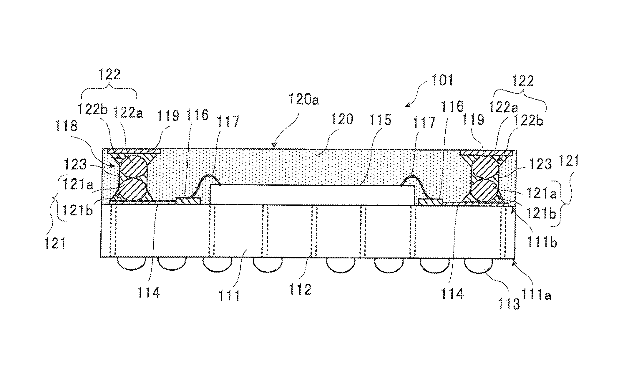
[0030]FIG. 1 is a longitudinal sectional view schematically illustrating a structure of a semiconductor package 101 according to a first embodiment of the present invention, and FIG. 2 is a plan view schematically illustrating a top view of the semiconductor package 101 according to the first embodiment. A package-on-package (POP) semiconductor device can be realized by stacking another package (not shown in the drawings) on the semiconductor package 101 according to the first embodiment.

[0031]As shown in FIG. 1 and / or FIG. 2, the semiconductor package 101 according to the first embodiment includes a wiring board (e.g., a glass epoxy substrate) 111 which has a wiring pattern (not shown in the drawings) formed by a printed wiring on a substrate and / or a through wiring 112 for electrically connecting both sides of the substrate by a through hole which penetrates the substrate, and a first electrode 113 for external connection (e.g., a solder terminal) which is disposed on a side of a ...

second embodiment

[0039]FIG. 6 is a longitudinal sectional view schematically illustrating a method of manufacturing a POP semiconductor device according to a second embodiment of the present invention, and FIG. 7 is a longitudinal sectional view schematically illustrating the POP semiconductor device according to the second embodiment. Elements in FIGS. 6 and 7 that are the same as or correspond to those in FIG. 1 are designated by the same reference numerals.

[0040]As shown in FIG. 6, in the method of manufacturing the POP semiconductor device according to the second embodiment, a first semiconductor package 101a is formed by the method of manufacturing the semiconductor package according to the first embodiment, a second semiconductor package 101b is formed by the method of manufacturing the semiconductor package according to the first embodiment, the second semiconductor package 101b is stacked on the first semiconductor package 101a so that the POP electrode 119 at the top of the first semiconduc...

third embodiment

[0043]FIG. 8 is a longitudinal sectional view schematically illustrating a structure of a POP semiconductor device according to a third embodiment of the present invention, and FIGS. 9A and 9B are diagrams of manufacturing steps schematically illustrating a method of manufacturing the POP semiconductor device according to the third embodiment. FIG. 10 is a plan view schematically illustrating a lead frame of the POP semiconductor device according to the third embodiment. Elements in FIGS. 8 and 9B that are the same as or correspond to those in FIG. 7 are designated by the same reference numerals.

[0044]As shown in FIG. 8, the POP semiconductor device according to the third embodiment has a structure that the POP semiconductor device according to the second embodiment shown in FIG. 7 is joined with a lead frame 140. As shown in the drawing, the lead frame 140 includes a mold resin 144 which covers a member 141 and a lead terminal 142 which is fixed outside of the mold resin 144, for e...


PUM


Abstract

A semiconductor package includes a wiring board; a first electrode for external connection; a ball pad; a semiconductor chip; a mold resin; an electrode unit connected with the ball pad and penetrating the mold resin; and a second electrode for external connection connected with a portion of the electrode unit on a side of an outer surface of the mold resin. The electrode unit includes a first ball disposed on the ball pad; a second ball disposed between the first ball and the second electrode; and a solder material connecting between the ball pad and the first ball, between the first ball and the second ball, and between the second ball and the second electrode for external connection; each of the first ball and the second ball including a core part having a glass transition temperature which is higher than a melting point of the solder material.

Description

BACKGROUND OF THE INVENTION[0001]1. Field of the Invention[0002]The present invention relates to a package-on-package (POP) semiconductor device, in which a semiconductor package is stacked on another semiconductor package and each of the semiconductor packages includes an internal semiconductor chip, a semiconductor package included in the POP semiconductor device, and methods of manufacturing them.[0003]2. Description of the Related Art[0004]There are various suggestions on POP semiconductor devices and semiconductor packages included in the POP semiconductor devices, for example, in Japanese Patent Kokai Publication No. 2008-16729 (Patent Document 1) and “Sanjigen jissou no PoP ni shin kouzou, teihaika to sekisoujiyuudo koujou wo jitsugen (a new structure of three-dimensional PoP which realizes to reduce package height and improve stacking flexibility)”, Nikkei Electronics of Jun. 16, 2008, pp. 12-13 (Non-Patent Document 1).[0005]Patent Document 1 (see FIG. 1 and claim 1, for exa...

Claims


Application Information

Patent Timeline
Patent Type & Authority Patents(United States)
IPC IPC(8): H01L23/498
CPCH01L21/568H01L23/3128H01L24/97H01L25/105H01L23/49816H01L23/49827H01L24/45H01L24/48H01L2224/45144H01L2224/48091H01L2224/48227H01L2224/49171H01L2224/97H01L2924/01004H01L2924/01013H01L2924/01029H01L2924/01078H01L2924/01079H01L2924/01082H01L2924/12044H01L2924/15311H01L2924/15312H01L2924/15331H01L2924/19043H01L2924/00014H01L2224/85H01L2924/01005H01L2924/01006H01L2924/01033H01L2924/014H01L24/49H01L2924/00H01L2225/1023H01L2225/1029H01L2225/1058H01L2924/01028H01L2924/181H01L2924/00012
Inventor EGAWA, YOSHIMI
Owner LAPIS SEMICON CO LTD
Why Eureka
Try Eureka