Integrated circuit

a technology of integrated circuits and integrated dies, applied in the field of integrated circuits, can solve the problems of pcb substrate routing difficulty, ribbon bonding may occupy more space on the ic die, and more expensive problems

Active Publication Date: 2012-11-27
SONY CORP
View PDF4 Cites 0 Cited by
  • Summary
  • Abstract
  • Description
  • Claims
  • Application Information

AI Technical Summary

Benefits of technology

[0006]1. is a simple and cheap solution using just bond-wire,

Problems solved by technology

However, this may be more expensive.
Moreover, ribbon bonding may occupy more space on IC die.
Also flip-chip connection may cause a routing difficulty between the IC die and PCB substrate (or interposer).
Thus this solution is not simple, low cost or small in footprint.

Method used


Image

  • Integrated circuit
  • Integrated circuit
  • Integrated circuit

Examples


Embodiment Construction

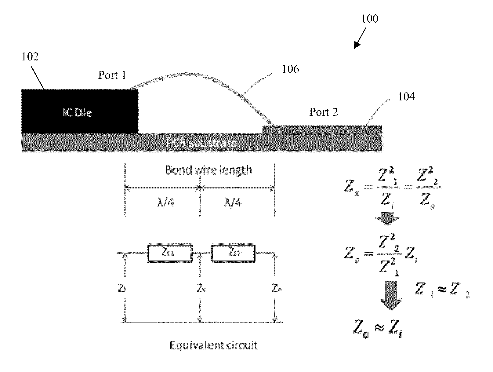
[0018]FIG. 1 shows an integrated circuit 100 including a die 102 connected to a PCB substrate (or its interposer coupler) 104 using a bond wire 106. The bond wire 106 is designed based on the quarter wavelength transformer theory. The input impedance for port 1 on the die 102 is Zi, the wavelength of the signal central frequency is λ and the characteristic impedance of the bond wire 106 is ZL, then after λ / 4 of the transmission line, the output impedance will be

[0019]Zo=ZL2Zi(1)

Symmetrically,

[0020]Zi=ZL2Zo(2)

[0021]The input impedance at port 1 is usually low, commonly 50 ohm or 75 ohm (corresponding to the characteristic impedance of the transmission line on the die 102). Since the wire is very thin, the transmission line built by bond wire has very high impedance. If port 1 on die or PCB is directly connected to bond wire, the impedance between the port and bond wire is mismatched, and the signal cannot pass through bond wire part well. If the impedance of the bond wire part can be...


PUM


Abstract

An integrated circuit comprising: a substrate; a first transmission line arranged on the substrate, the first transmission line having a first termination; a die having a first surface on the substrate and an opposed second surface, the die being spaced from the first termination; a second transmission line arranged on the second surface of the die, the second transmission line having a second termination; and a bond wire connected between the first termination and the second termination configured to have a length half the wavelength of the signal central frequency.

Description

CROSS REFERENCE TO RELATED APPLICATIONS[0001]The present application contains subject matter related to that disclosed in Singapore Priority Patent Application 200905866-0 filed in the Singapore Patent Office on Sep. 2, 2009, the entire content of which is hereby incorporated by reference.FIELD OF THE INVENTION[0002]The present invention relates to an integrated circuit, particularly though not solely, to a wire bond connection between components in a high frequency integrated circuit.BACKGROUND[0003]Bonding wire is a widely used connection approach between an IC die and a substrate or PCB. Bond wires are very simple, convenient and low cost. However, it is usually considered as a low frequency approach. In a high frequency IC, such as 60 GHz millimeter frequency band, typically ribbon bonding or flip-chip bonding is used because those connections have lower inductance and better high frequency performance. However, this may be more expensive. Moreover, ribbon bonding may occupy mor...

Claims


Application Information

Patent Timeline
Patent Type & Authority Patents(United States)
IPC IPC(8): H01L23/66H03H7/38
CPCH01P5/028H01L2924/3011H01L2224/48227H01L2924/30107H01L2224/48091H01L2924/00014H01L2924/00
Inventor MA, YUGANGSUN, XIAOBING
Owner SONY CORP
Why Eureka
Try Eureka