
Processes for enhanced 3D integration and structures generated using the same

a technology of enhanced electronic 3d and integration, applied in the direction of solid-state devices, basic electric elements, electrical apparatus construction details, etc., can solve the problems of low input/output density, signal delay, and difficulty in powering the system through edge connections, and achieve the effect of enhanced 3d integration

Active Publication Date: 2012-12-11
INT BUSINESS MASCH CORP
View PDF51 Cites 2 Cited by
  • Summary
  • Abstract
  • Description
  • Claims
  • Application Information

AI Technical Summary

Benefits of technology

The 4DI approach enhances memory content accessibility by 10-fold within a single processor clock-cycle, achieves high communication bandwidth, and addresses cooling and ESD protection challenges, while simplifying the integration process and reducing parasitics and heat dissipation issues.

Problems solved by technology

The so-called “cube” structures described in these references is a result of a procedure also known in the art as chip stacking, but this has several drawbacks that include inter alia; edge connection architecture which leads to signal delay, lower input / output (I / O) density, difficulty in powering the system through edge connections, and difficulty in cooling the system for high power use.
Scaling of complementary metal-oxide-semiconductors (CMOS) transistor devices to smaller and smaller dimensions to enable larger circuit density is running into challenges in that the performance of such ultra small devices is not scaling favorably due to short channel effects in the device behavior, the difficulty in scaling channel strain induced mobility enhancements and the like.
First, additional memory needs to be located close to the logic circuitry with fast access time and second, high bandwidth interconnects are required for the logic circuits to send and retrieve information from these memory cells on the chip thus driving a huge increase in interconnect density and speed.
Thus more clock-cycles are needed to access them during complex operations requiring a large amount of memory to be retrieved, processed, and stored back.
As these components are typically fabricated on different substrates using processes which may be incompatible with currently practiced silicon CMOS processes, they cannot be embedded into a silicon chip using 2D process methodologies.
Thus such components tend to be integrated with CMOS using chip carriers or circuit boards as a means to interconnect them which can limit the ability to fully utilize the capability of the components.
Due to such a connection scheme, chip-level connection typically enables more content than 2D but the access time between devices is limited by inductive and capacitive delays associated with the bonded wire connections and going to the edges of the chips.
Also it is difficult to conveniently deliver power to the various chips in the stacked assembly.
In all 3DI integration schemes mentioned above, the cooling of the system is typically a difficult issue to resolve.
Provision of micro-channels for cooling on the bulk silicon substrate of the assembly in the final 3DI stack can provide enhanced cooling but cannot completely achieve an effective cooling of upper layers when many device layers are stacked in the 3D system.
This limits the number of 3DI devices stackable into a system as the heat dissipation becomes a road block for further 3D content increase.
Another issue associated with 3DI is the thru-Si connection electro-static discharge (ESD) protection requirements.
This can be a large load as the number of devices increases and requires a large driver to access the 3DI circuits which could significantly slow them down.
In general, the current thru-Si 3D wafer stacking processes and resultant devices present many processing related issues, e.g., thin Si construction (<100 um) requires stacking wafers one at a time to allow thru-Si vias; it is difficult to make the via less than 5 um in size and 10 um in pitch in devices employing Cu; thru-Si vias can be made from W but W has a higher resistivity than Cu; thru-Si vias pass through the bonding interface making bonding defects difficult to control; wafer stacks are limited due to bonding thermal cycles; the process is complex and introduces via yield and wafer yield issues; manufacturing involves long process cycles; wafer level distortions are introduced.
Accommodation of thru-Si vias requires significant changes in the lay out of processor and memory chips in addition to leading to loss of useable silicon area available for device circuits.
The chip cube approaches known in the current art which avoid thru-Si via related concerns, however are limited in their ability to provide a high bandwidth for data communication in and out of the structure and have high parasitics as they depend on edge leads or wire bonds formed after assembly.

Method used


Image

  • Processes for enhanced 3D integration and structures generated using the same
  • Processes for enhanced 3D integration and structures generated using the same
  • Processes for enhanced 3D integration and structures generated using the same

Examples


Embodiment Construction

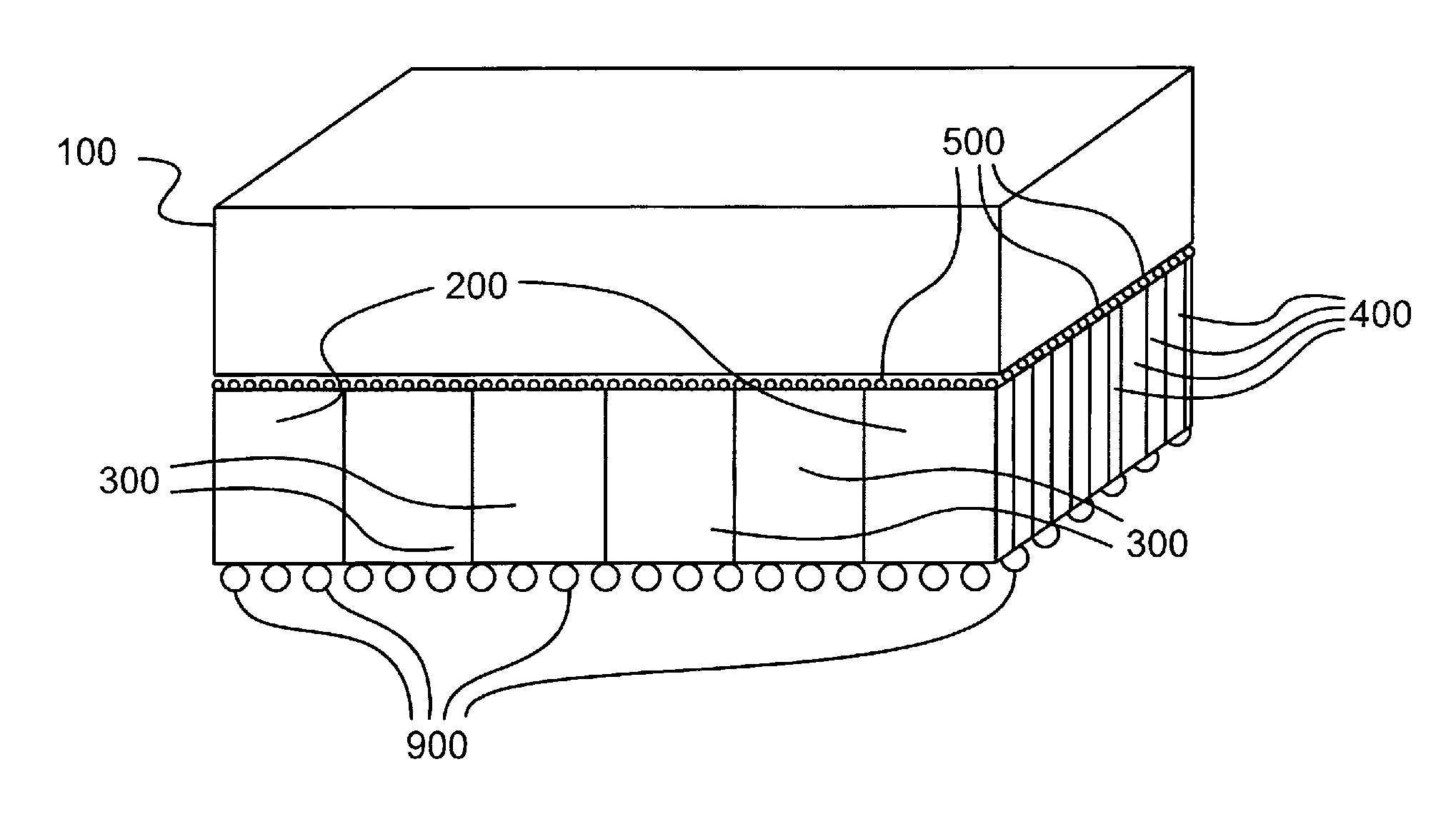
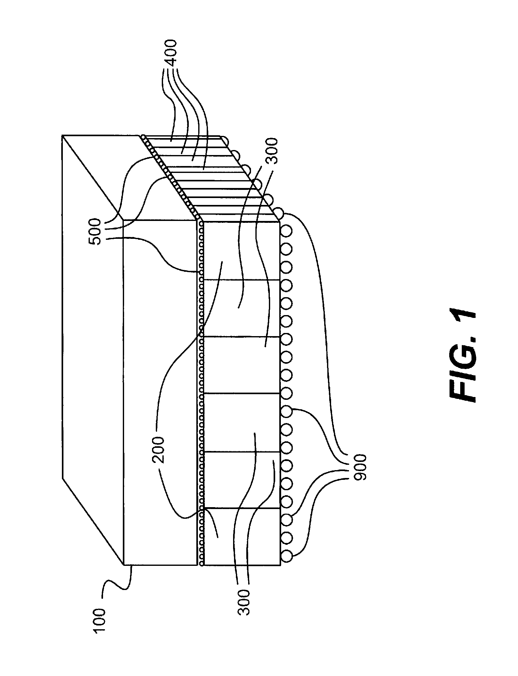
[0032]FIG. 1 shows a schematic isometric view of a 4DI final assembly comprising a logic microprocessor chip 100 attached to a collection of vertically stacked slices 200 and 300 through microjoints 500. Slices 200 and 300 are typically slices from memory wafers but in one later embodiment the end slices 200 are chosen to be slices from an optoelectronic device wafers. The view also shows the metal wiring lines 400 running along the vertical face of one of the end slices 200 and these lines are connected to circuitry present in the slice. Although the lines are shown only on this end slice for clarity, such lines are provided on the active surface of all of the slices 200 and 300. At the bottom of the slice stack an array of C4 solder joints 900 are shown which enable attaching the whole 4DI assembly to a packaging substrate (not shown). Microjoints 500 and C4 solder joints 900 connect to metallization patterns (omitted in FIG. 1 for clarity) located on the top and bottom surfaces o...


PUM


Abstract

An enhanced 3D integration structure comprises a logic microprocessor chip bonded to a collection of vertically stacked memory slices and an optional set of outer vertical slices comprising optoelectronic devices. Such a device enables both high memory content in close proximity to the logic circuits and a high bandwidth for logic to memory communication. Additionally, the provision of optoelectronic devices in the outer slices of the vertical slice stack enables high bandwidth direct communication between logic processor chips on adjacent enhanced 3D modules mounted next to each other or on adjacent packaging substrates. A method to fabricate such structures comprises using a template assembly which enables wafer format processing of vertical slice stacks.

Description

STATEMENT PURSUANT TO 37° C.F.R. §1.77 (B) (3) REGARDING FEDERALLY SPONSORED RESEARCH OR DEVELOPMENT[0001]This invention was made under a federally sponsored research and development agreement, H98230-08-C-1468, “CYCLOPS II ARCHITECTURE and ENGINEERING STUDY.”FIELD OF THE INVENTION[0002]The field of the invention comprises integrated electronic 3D system devices and a process for building integrated 3D system devices that enables a higher level of system integration than possible with current 3D integration processes and structures, but does not employ through silicon vias.BACKGROUND OF THE INVENTION AND RELATED ART[0003]Various processes and structures described in the related art address high level system integration such as Hoffman, et al., U.S. Pat. No. 6,033,931, one of a class of so-called “cube patents.” Hoffman, et al. discloses a three-dimensional microchip circuit assembly process that employs a three-layer dry film sandwich to prepare a stacked circuit cube. Bertin, et al...

Claims


Application Information

Patent Timeline
Patent Type & Authority Patents(United States)
IPC IPC(8): H01L23/02
CPCB23P11/00H05K1/11H05K1/14H05K7/00H01L23/49816H01L21/78Y10T29/49826H01L2924/0002H01L2924/00H01L25/50H01L25/0657H01L2924/14H01L2223/54426H01L23/544H01L2924/01079H01L2225/06513H01L2225/06551H01L2924/01029
Inventor COLGAN, EVAN G.PURUSHOTHAMAN, SAMPATHYU, ROY R.
Owner INT BUSINESS MASCH CORP
Learn More