Holographic microscopy of holographically trapped three-dimensional nanorod structures

a three-dimensional nanorod and holographic microscopy technology, applied in the field of holographic microscopy of holographically trapped three-dimensional nanorod structures, can solve the problems of reducing imaging speed, adding substantial complexity, and no complementary method in the prior art for examining optically trapped structures

Active Publication Date: 2012-12-11
NEW YORK UNIV
View PDF13 Cites 35 Cited by
  • Summary
  • Abstract
  • Description
  • Claims
  • Application Information

AI Technical Summary

Problems solved by technology

No complementary method has been available in the prior art for examining optically trapped structures except for conventional two-dimensional microscopy.
The trapping pattern would have to be translated to compensate for the microscope's mechanical motion, which would add substantial complexity, would greatly reduce imaging speed, and would likely disrupt the sample undergoing examination and analysis.
The high-numerical-aperture optics required for such studies offer optimal spatial resolution, but severely restrict the accessible depth of focus to within a few micrometers.
Scanning takes time, however, and so is of limited utility for studying the dynamic processes that evolve in three dimensions.
Some implementations also require the sample to be fluorescently labeled, which may not be desirable.
Scanning probe microscopy and electron microscopy both have superior spatial resolution, but typically are not compatible with three-dimensional micromanipulation techniques, particularly under environmental conditions.

Method used


Image

  • Holographic microscopy of holographically trapped three-dimensional nanorod structures
  • Holographic microscopy of holographically trapped three-dimensional nanorod structures
  • Holographic microscopy of holographically trapped three-dimensional nanorod structures

Examples


Embodiment Construction

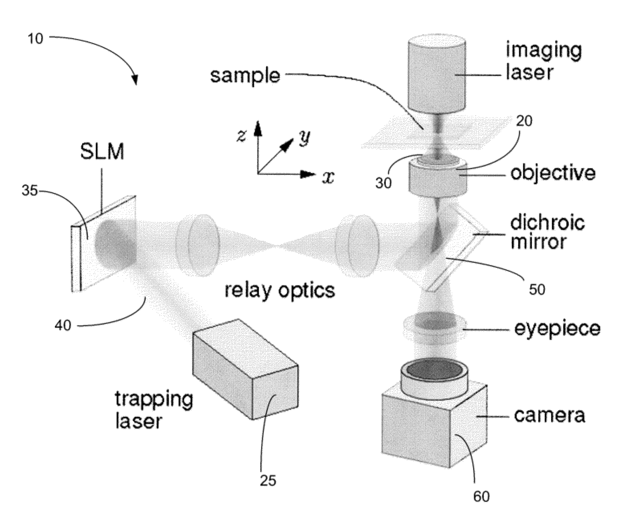
[0016]FIG. 1 shows a schematic representation of an integrated system 10 constructed in accordance with one embodiment of the invention. The system 10 is based on an inverted optical microscope (such as, Zeiss Axiovert S100-TV) outfitted with a 100× NA 1.4 oil immersion objective lens 20. This lens 20 is used both to project holographic optical traps, and also to collect in-line holographic images of trapped objects. Holographic traps are preferably powered by a frequency-doubled diode-pumped solid state laser 25 (such as, a Coherent Verdi) operating at a wavelength of 532 nm to generate input laser beam 30. A liquid crystal spatial light modulator 35 (such as a Hamamatsu PAL-SLM X7550) imprints the beam's wavefronts with phase-only holograms encoding the desired trapping pattern. The modified trapping beam 40 then is relayed to the input pupil of the objective lens 20 and is focused into optical traps.

[0017]The trapping beam 40 is preferably relayed to the objective lens 20 with a ...


PUM


Abstract

A method and system for performing three-dimensional holographic microscopy of an optically trapped one dimensional structure. The method and system use an inverted optical microscope, a laser source which generates a trapping laser beam wherein the laser beam is focused by an objective lens into a plurality of optical traps. The method and system also use a collimated laser at an imaging wavelength to illuminate the structure created by the optical traps. Imaging light scattered by the optically tapped structure forms normalized intensity holograms that are imaged by a video camera and analyzed by optical formalisms to determine light field to reconstruct 3-D images for analysis and evaluation.

Description

CROSS REFERENCE TO RELATED PATENT APPLICATIONS[0001]The present application is a continuation-in-part of U.S. Utility application Ser. No. 12 / 020,376 filed Jan. 25, 2008, which claims the benefit of priority to U.S. Provisional Patent Application 60 / 897,784 filed Jan. 26, 2007, both of which are incorporated by reference herein in their entirety.[0002]The U.S. Government has certain rights in this invention pursuant to grants from the National Science Foundation through Grant Number DBI-0629584 and Grant Number DMR-0606415.[0003]This invention is directed to a holographic optical trapping system using optical traps generated by computer-established holograms to organize materials and apply microscope optics to inspect and analyze the materials in three dimensions (3-D). More particularly, a holographic video microscope system uses real-time resolved volumetric images of 3-D microstructures to carry out tracking and inspection of material assemblies, including 3-D translational and r...

Claims


Application Information

Patent Timeline
Patent Type & Authority Patents(United States)
IPC IPC(8): G02B21/00
CPCG01B9/021G02B21/32G03H1/0005G03H1/0443G03H1/0866G02B21/0088G03H1/2294G03H2001/0033G03H2001/0077G03H2001/0447
Inventor CHEONG, FOOK CHIONGGRIER, DAVID G.LEE, SANG-HYUK
Owner NEW YORK UNIV
Why Eureka
Try Eureka