Semiconductor integrated circuit and electronic device

a technology of integrated circuits and semiconductors, applied in the direction of electric variable regulation, process and machine control, instruments, etc., can solve the problems of one type of sensor circuits and the determination of the magnitude of uncertainty of gate delay, and achieve the effect of being ready to us

Active Publication Date: 2012-12-25
RENESAS ELECTRONICS CORP
View PDF2 Cites 6 Cited by
  • Summary
  • Abstract
  • Description
  • Claims
  • Application Information

AI Technical Summary

Problems solved by technology

The first problem is that one type of sensor circuits are used to detect both of variability (mean value) and uncertainty (standard deviation σ).
The second problem is that the magnitude of uncertainty of gate delay is determined outside the chip.
The last problem is that when determining the variability (mean value) of gate delay and the uncertainty (standard deviation σ) thereof to derive an optimum voltage, only the sum of the mean value and 3σ—the standard deviation σ multiplied by three—is taken into account as the worst value of data path delay, simply.

Method used


Image

  • Semiconductor integrated circuit and electronic device
  • Semiconductor integrated circuit and electronic device
  • Semiconductor integrated circuit and electronic device

Examples


first embodiment

[0075]>

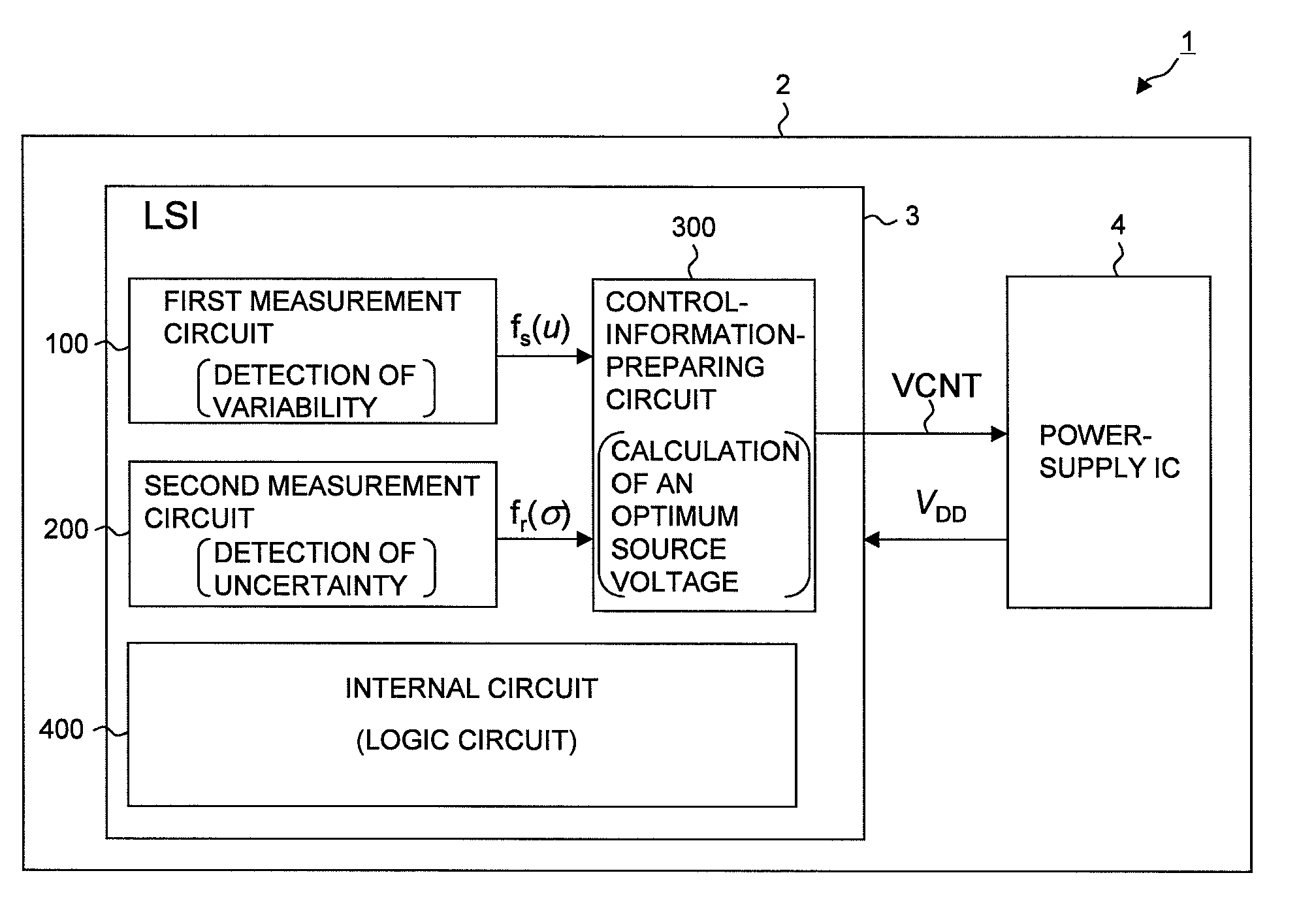
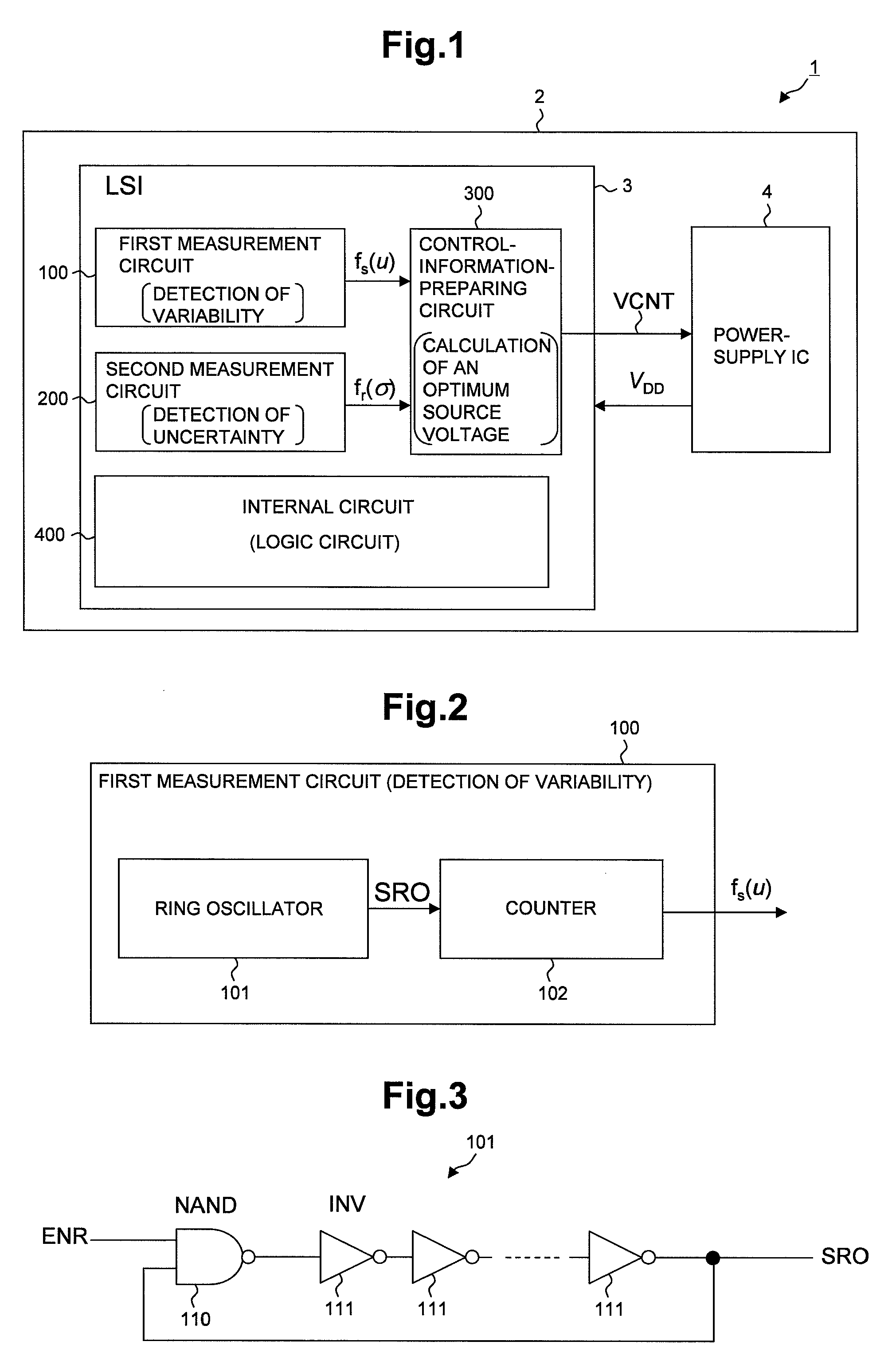
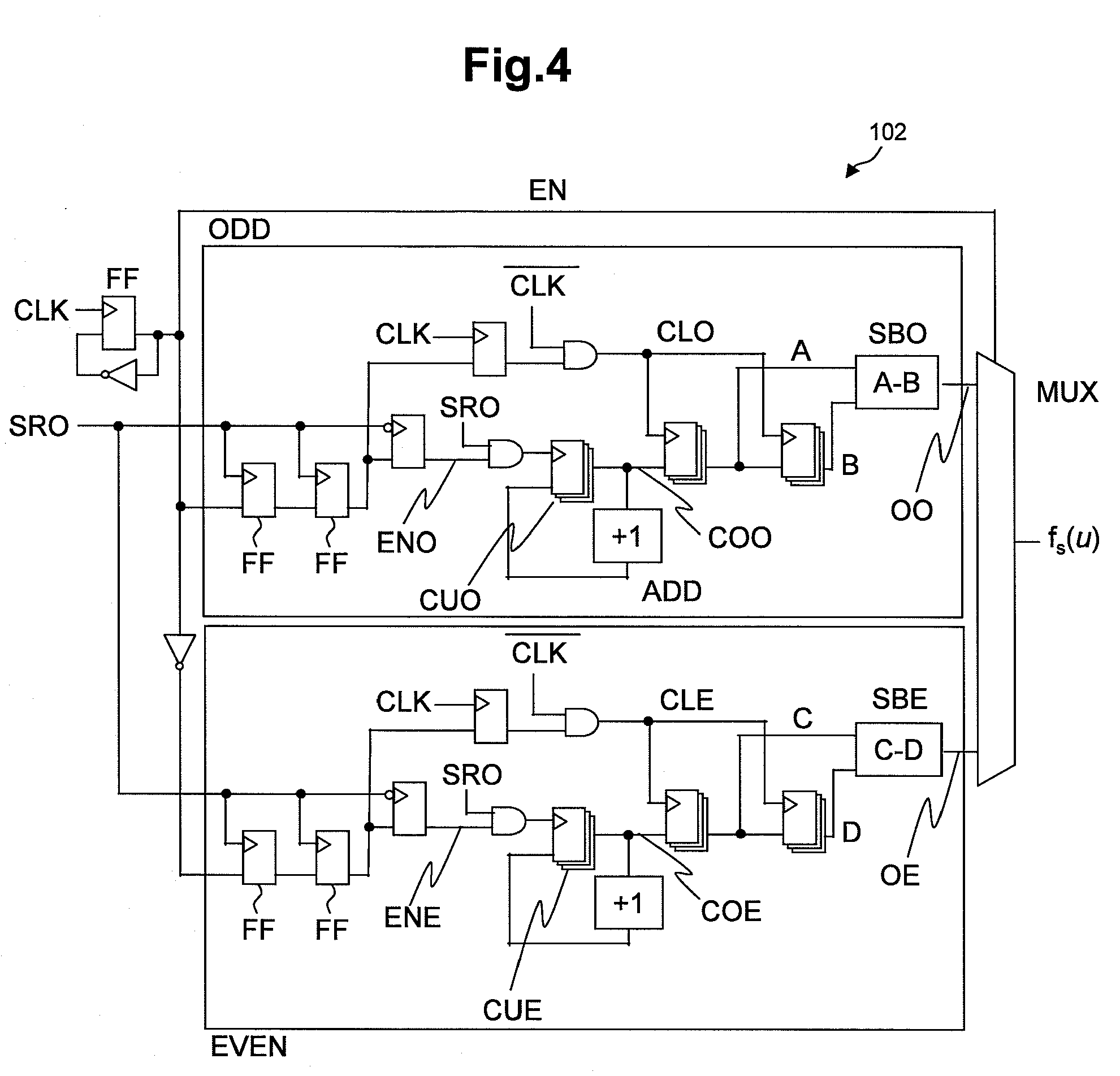
[0076]FIG. 1 shows an example of the configuration of a system associated with the first embodiment, which executes an adaptive voltage scaling according to the magnitudes of variability and uncertainty—different types of process variations.

[0077]The system shown in the drawing is composed of an electronic device 1 including: a semiconductor integrated circuit (LSI) 3 with a number of gates provided therein; a power-supply IC 4 serving as a power-source circuit operable to supply an electric power to LSI 3; and a mounting board 2 on which the power-supply IC 4 is mounted. While only one LSI 3 is shown in the drawing, it typifies more than one LSI. Actually, two or more LSIs required for realizing a given function may be disposed. In such case, the power-supply IC 4 supplies a supply voltage to the LSIs, and what is targeted for adaptive supply-voltage control may be part or all of LSIs. In the case of part of LSIs targeted for adaptive supply-voltage control, a predetermined ...

second embodiment

[0118]FIGS. 14 and 15 show other examples of the first measurement circuit for determining a relative value of the variability, and the second measurement circuit for determining a relative value of the uncertainty respectively, which are involved in a system according to the second embodiment of the invention.

[0119]The system according to the second embodiment has the feature that more than one ring oscillator is placed in each of the first and second measurement circuits 100m and 200m corresponding to more than one typical type of logic gates used in the internal circuit 400. Usually, more than one type of gates are incorporated in a logic circuit, and the variability and uncertainty of values of delays of the gates differ from each other in quantity. Therefore, it is preferable that the same number of ring oscillators as the number of the types of logic gates are prepared to sense variations for each gate. By making such arrangement, the timing of an action of an actual semicondu...

third embodiment

[0123]FIG. 16 shows an example of a correspondence table 304 involved in a system according to the third embodiment of the invention; the correspondence table is stored in the storing unit 301 of the control-information-preparing circuit 300, and presents correspondences between performances required of chips, and variations of the variability and uncertainty corresponding to the required performances. FIG. 17 shows an example of the operation flow of the adaptive voltage scaling through the use of a feedback loop using the correspondence table 304 shown by FIG. 16. The system according to the third embodiment is different from the systems according to the first and second embodiments in the structure of the correspondence table stored in the storing unit 301, and the detail of the processing for AVS (Adaptive Voltage Scaling), which the control-information-preparing circuit 300 executes. A feature which the system according to the third embodiment has is as follows. While the semic...


PUM


Abstract

AVS (Adaptive Voltage Scaling) technique, by which variability and uncertainty are both taken into account. In the system arranged for AVS technique, a detection circuit optimum for each type of process variation is set. Examples of the detection circuit so arranged include a first measurement circuit for detection of variability, which produces a relative value with respect to the gate delay mean value, and a second measurement circuit for detection of uncertainty, which produces a relative value related to the gate delay standard deviation. The first and second measurement circuits are provided separately from each other. The control information for deciding the supply voltage is prepared based on relative values produced by the detection circuits. When preparing the control information, reference is made to e.g. a table data.

Description

CLAIM OF PRIORITY[0001]The Present application claims priority from Japanese application JP 2010-013304 filed on Jan. 25, 2010, the content of which is hereby incorporated by reference into this application.FIELD OF THE INVENTION[0002]The present invention relates to a semiconductor integrated circuit and an electronic circuit having the same. Particularly it relates to an AVS (Adaptive Voltage Scaling) technique for controlling a supply voltage to correct the fluctuation of the operation speed owing to the gate delay.BACKGROUND OF THE INVENTION[0003]For reduction in power consumption demanded of SoC (System On a Chip) used in mobile phones, it is important to lower a supply voltage. However, with the scale-down of semiconductor processes, the leak current and process variations increase, and it is becoming difficult to lower the supply voltage. Under the circumstances, the AVS technique which enables each chip to be supplied with an optimum supply voltage depending on the process v...

Claims


Application Information

Patent Timeline
Patent Type & Authority Patents(United States)
IPC IPC(8): G05F1/10
CPCG01R31/31725G01R31/3004H01L2924/0002H01L2924/00
Inventor OTSUGA, KAZUOKANNO, YUSUKETAKAZAWA, YOSHIO
Owner RENESAS ELECTRONICS CORP
Why Eureka
Try Eureka