Optical device having extented depth of field and fabrication method thereof

a technology of optical imaging and depth of field, applied in the field of optical imaging devices with increased depth, can solve the problems of reducing the optical efficiency of the optical imaging system, lens aberration, misfocus errors,

Active Publication Date: 2013-01-08
VISERA TECH CO LTD +1
View PDF9 Cites 11 Cited by
  • Summary
  • Abstract
  • Description
  • Claims
  • Application Information

AI Technical Summary

Benefits of technology

[0002]The invention relates to an optical device for reducing image errors and more particularly to an optical device with increased depth of field and method for fabricating the same.

Problems solved by technology

The errors or distortions introduced by the optical devices may include lens aberrations, such as non-rotationally symmetrical aberrations (e. g. coma or astigmatism aberrations) and rotationally symmetrical aberrations (e.g. spherical aberrations), and misfocus errors resulting from an object being located away from the position of best focus.
However, increasing the lens F-number may reduce the optical efficiency of the optical imaging system.
Generally, a complicated lens system is capable of greatly expanding the depth of field, but is very expensive.
However, since the phase mask needs to be implemented with a non-rotational surface with high accuracy, fabrication thereof is very difficult.
Namely, fabrication errors increase for phase masks having complicated contours resulting in increased failures for subsequent image restoration processes, thus, increasing fabrication costs for camera module.

Method used


Image

  • Optical device having extented depth of field and fabrication method thereof
  • Optical device having extented depth of field and fabrication method thereof

Examples


Embodiment Construction

[0013]The following description is of the best-contemplated mode of carrying out the invention. This description is provided for the purpose of illustrating the general principles of the invention and should not be taken in a limiting sense. The scope of the invention is best determined by reference to the appended claims.

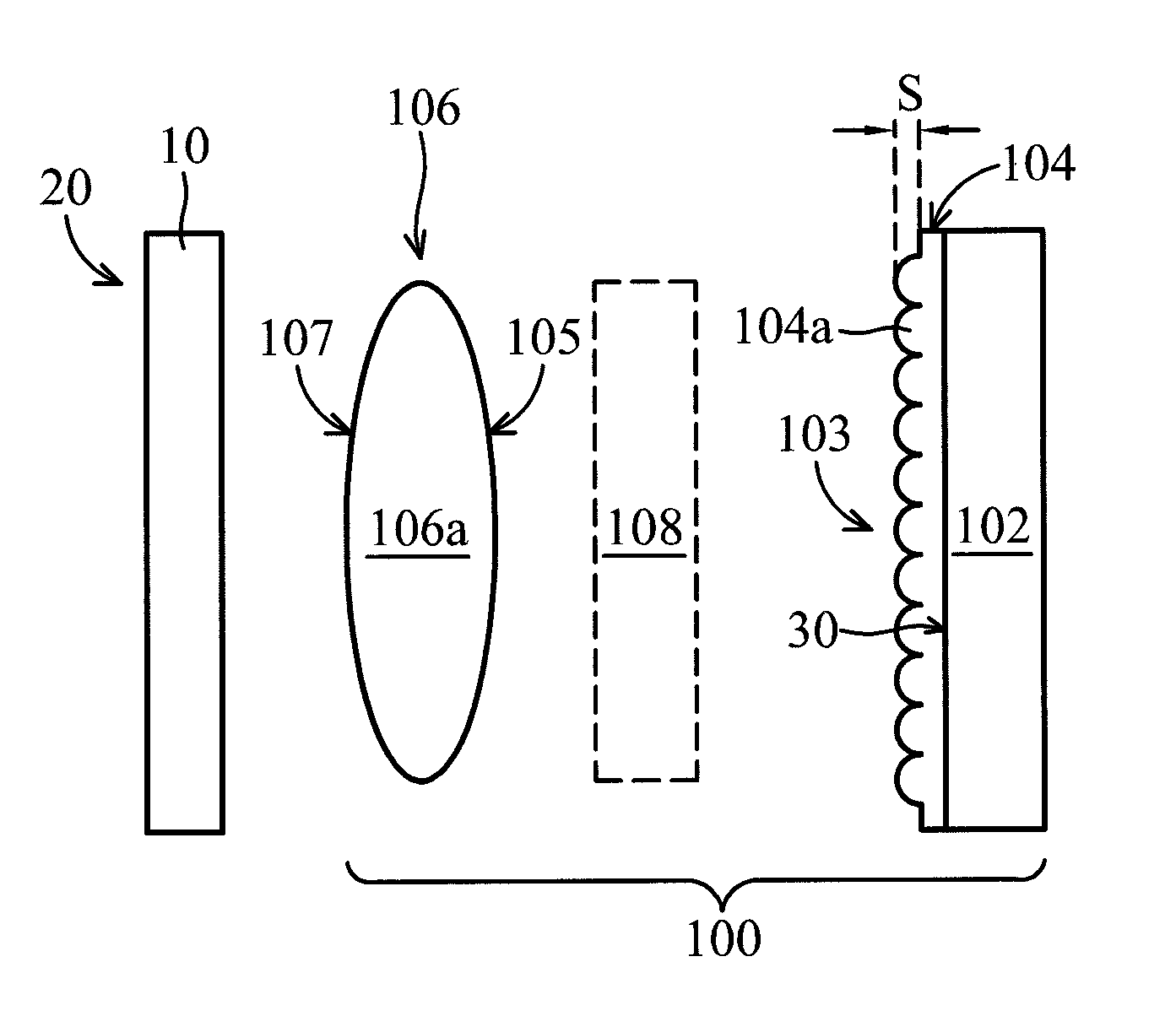
[0014]FIG. 1 illustrates an exemplary embodiment of an optical device 100 according to the invention. In the embodiment, the optical device 100, such as a digital camera, may comprise an image sensor device 102 and a lens module 106 constituted by at least one lens 106a and disposed above the image sensor device 102. The image sensor device 102 has a microlens array 104 thereon and corresponding to a pixel array (not shown) therein. Namely, each microlens in the microlens array 104 corresponds to each image sensor in the pixel array. The image sensor device 102 may be a charge coupled devices (CCD) or complementary metal oxide semiconductor (CMOS) type image sensor...


PUM


Abstract

A method for designing an optical device which includes a lens and a microlens array is disclosed. A point spread function (PSF) of the lens including rotationally symmetrical aberration coefficients is formulated, wherein the PSF presents various spherical spot sizes. A virtual phase mask having phase coefficients is provided and the phase coefficients are added to the PSF of the lens, such that the various spherical spot sizes are homogenized. The virtual phase mask is transformed into a polynomial function comprising high and low order aberration coefficients. A surface contour of the lens is determined according to the rotationally symmetrical aberration coefficients and the low order aberration coefficients, and a sag height of each microlens in the microlens array is determined according to the high order aberration coefficients. An optical device using the design method is also disclosed.

Description

BACKGROUND OF THE INVENTION[0001]1. Field of the Invention[0002]The invention relates to an optical device for reducing image errors and more particularly to an optical device with increased depth of field and method for fabricating the same.[0003]2. Description of the Related Art[0004]Improving optical imaging systems to obtain images that are free of errors or distortions introduced by optical devices used in optical imaging systems has long been a goal in the development of optical imaging technology. The errors or distortions introduced by the optical devices may include lens aberrations, such as non-rotationally symmetrical aberrations (e. g. coma or astigmatism aberrations) and rotationally symmetrical aberrations (e.g. spherical aberrations), and misfocus errors resulting from an object being located away from the position of best focus.[0005]One approach to reduce such imaging errors or distortions introduced by the optical devices is to increase the lens F-number (which is ...

Claims


Application Information

Patent Timeline
Patent Type & Authority Patents(United States)
IPC IPC(8): G02B27/10
CPCG02B27/0012G02B27/0075G02B27/0025
Inventor DENG, JAU-JANKAO, YU-SHUHSU, YUN-CHIANG
Owner VISERA TECH CO LTD
Why Eureka
Try Eureka