Semiconductor wafer metrology apparatus and method

a technology of semiconductor wafers and metrology, applied in the field of semiconductor wafer metrology, can solve problems such as residual charge and errors, and achieve the effects of reducing air current effects, limiting effect, and reducing electrostatic force

Inactive Publication Date: 2013-01-22
METRYX
View PDF29 Cites 11 Cited by
  • Summary
  • Abstract
  • Description
  • Claims
  • Application Information

AI Technical Summary

Benefits of technology

[0008]The current invention seeks to build on the measurement technique disclosed in WO 02 / 03449. The inventor has found that when performing sensitive mass measurements on wafers where atmospheric buoyancy is eliminated or suitably compensated other (typically smaller) errors become noticeable. For example, such errors may be caused by pressure effects due to atmospheric movement (air currents) around the wafer and electrostatic forces due to charges on the wafer or surrounding materials. WO 02 / 03449 noted that these effects were minor compared with atmospheric buoyancy and proposed to limit their effect by performing the weight measurement in a housing (weighing chamber). The chamber was sized to strike a balance between providing a small space to reduce air current effects and spacing surrounding materials far enough away from the wafer to reduce the effect of electrostatic forces. These are conflicting requirements. The present invention proposes a solution which can enable both effects to be reduced.
[0011]Semiconductor wafers are typically thin disks (e.g. 200 or 300 mm in diameter and 1 mm thick). This means the majority of any electrostatic force acts normal to the plane of the wafer, e.g. the electrostatic force between a chamber wall and a wafer can be compared with the force between plates in a parallel plate capacitor. By changing the orientation of the wafer from horizontal to vertical or near vertical, the surface area in the direction of a force (weight) sensor is reduced. Hence, the electrostatic force components acting in the same direction as the wafer weight force component is reduced.
[0015]Since the electrostatic force is reduced by effectively redirecting its force components (rather than reducing the size of those components), the chamber can form a smaller enclosure for the wafer. The effects of air currents in the chamber may therefore also be reduced.
[0016]Moreover, since an upright wafer presents a smaller cross-section to the weighing instrument in the direction of its weight force. This means that the effect on the weight measurement of components of air current in that direction can be reduced, e.g. since the size of the error force may be proportional to the area on the wafer on which the air current acts.
[0020]In this context, substantially upright preferably means within 10°, more preferably 5°, from vertical (aligned with the force of gravity). In fact a small non-zero angle to exact vertical may be desirable to improve wafer stability during weight measurement. Accordingly, the wafer holder preferably includes a base for supporting a lower edge of the wafer in the upright orientation, and a upstanding backrest for supporting an upper part of the wafer such that the upright orientation is a small non-zero angle from exact vertical. The base may have a lip to prevent the wafer from slipping.

Problems solved by technology

For example, such errors may be caused by pressure effects due to atmospheric movement (air currents) around the wafer and electrostatic forces due to charges on the wafer or surrounding materials.
However, they are limited because they can only neutralise surface charges and often have unbalanced positive and negative ion streams, which causes them to leave a residual charge.

Method used


Image

  • Semiconductor wafer metrology apparatus and method
  • Semiconductor wafer metrology apparatus and method
  • Semiconductor wafer metrology apparatus and method

Examples


Embodiment Construction

; FURTHER OPTIONS AND PREFERENCES

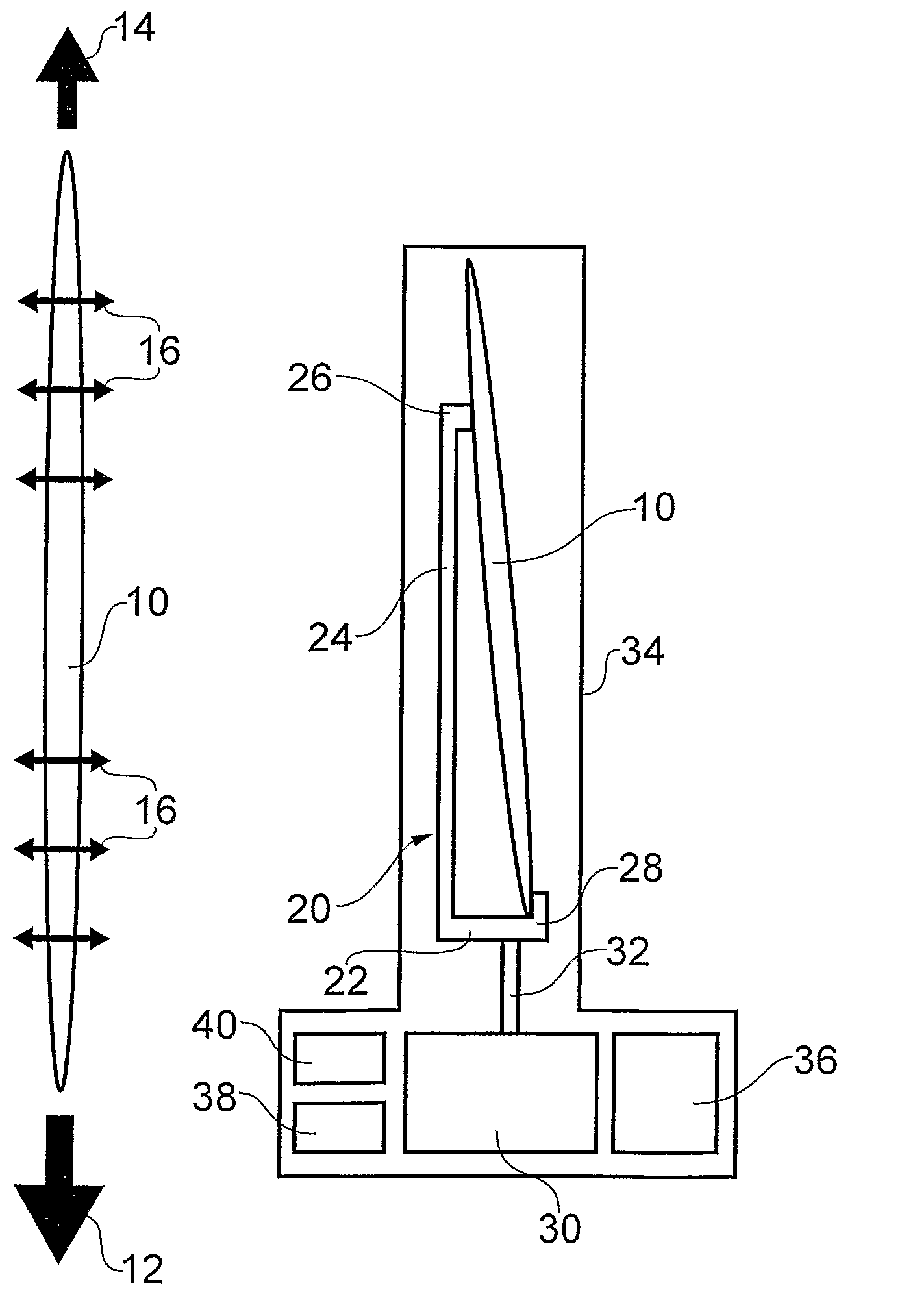
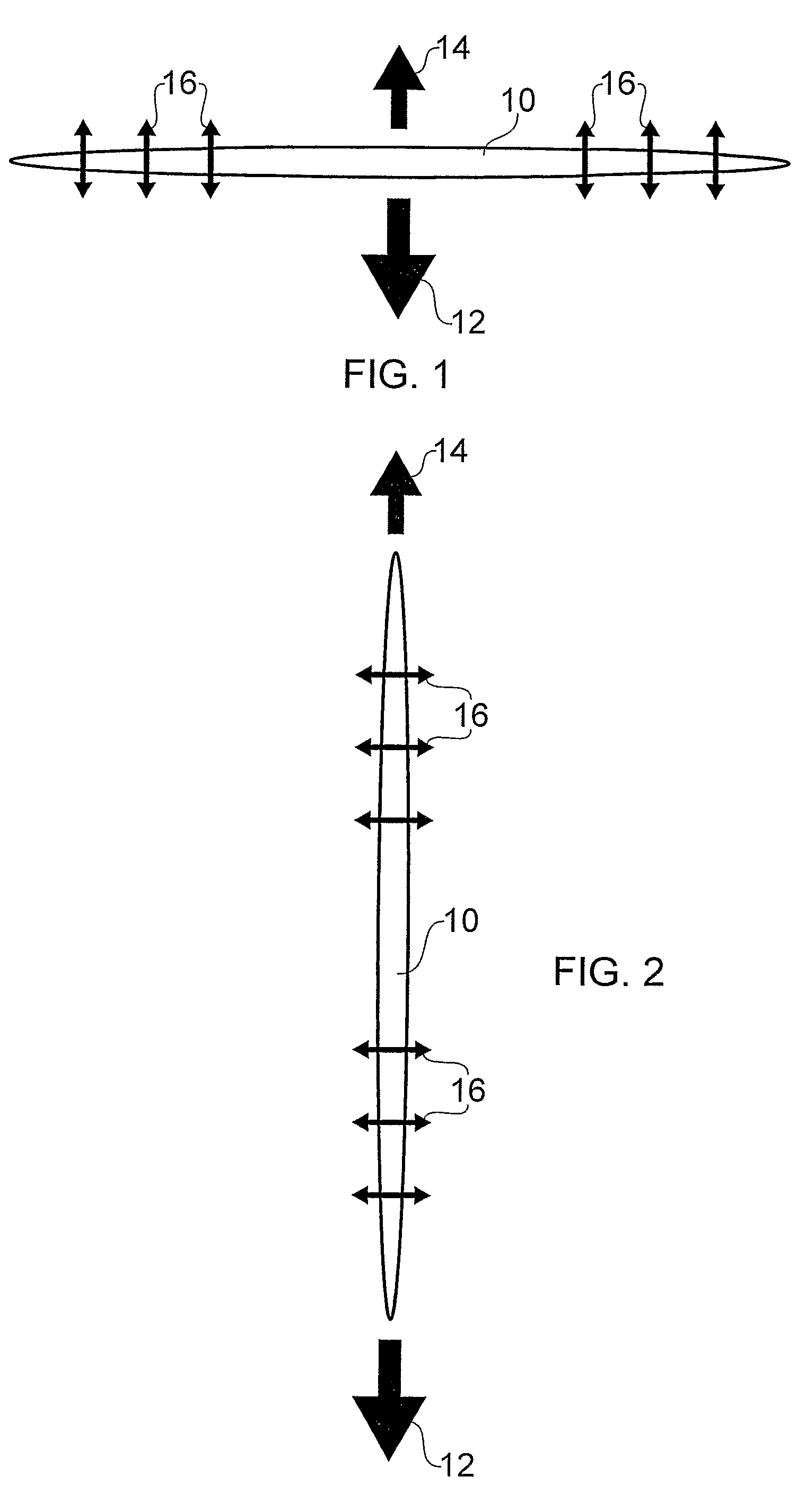
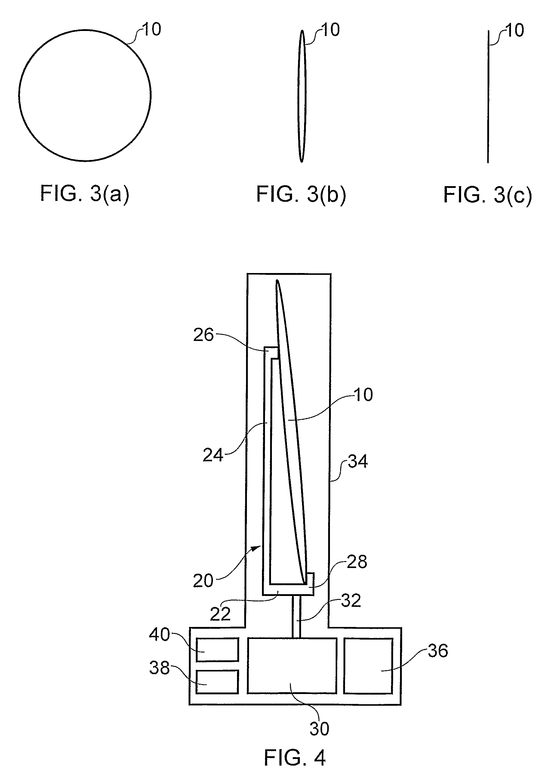
[0031]FIGS. 1 and 2 demonstrate the theory behind the invention. FIG. 1 shows some of the forces experienced by a semiconductor wafer 10 in a non-evacuated chamber (not shown) during weight measurement. The weight force 12 due to gravity is counteracted by an atmospheric buoyancy force 14. This buoyancy force 14 can be detected and compensated for in a weight measurement. However, there are additional (smaller) electrostatic forces 16 which also act substantially parallel to the weight force. When the buoyancy force 14 is compensated for, these electrostatic forces 16 can cause a noticeable error in the weight measurement. The electrostatic forces 16 are caused by interaction between the walls of the chamber and the wafer. The geometry of the wafer means that these forces are predominantly normal to the plane of the wafer 10.

[0032]FIG. 2 demonstrates that if the wafer 10 is held in an upright orientation, the electrostatic forces 16 are rotated out o...


PUM


Abstract

A semiconductor wafer metrology technique comprising performing atmospheric buoyancy compensated weighing of a wafer, in which the wafer is weighed in a substantially upright condition. A vertical or near vertical wafer orientation causes the surface area in the direction of a force (weight) sensor to be reduced compared with a horizontal wafer orientation. Hence, the electrostatic force components acting in the same direction as the wafer weight force component is reduced.

Description

TECHNICAL FIELD[0001]This invention relates to semiconductor wafer metrology.BACKGROUND TO THE INVENTION[0002]Microelectronic devices are fabricated on semiconductor wafers using a variety of techniques, e.g. including deposition techniques (CVD, PECVD, PVD, etc) and removal techniques (e.g. chemical etching, CMP, etc). Semiconductor e.g. silicon wafers may be further treated in ways that alter their mass e.g. by cleaning, ion implantation, lithography and the like. These treatment techniques typically cause a change in the mass at or on the surface of the semiconductor wafer. The configuration of the changes to the surface are often vital to the functioning of the device, so it is desirable for quality control purposes to assess wafers during production in order to determine whether they have the correct configuration.[0003]A number of existing measurement techniques are known. For etching treatment, one known technique is to break a treated wafer and perform a detailed analysis of...

Claims


Application Information

Patent Timeline
Patent Type & Authority Patents(United States)
IPC IPC(8): H01L21/66G01R31/26
CPCG01G21/28G01G23/01G01G21/22G01G23/16G01G9/00H01L21/67253H01L22/12
Inventor WILBY, ROBERT JOHN
Owner METRYX
Why Eureka
Try Eureka