Electrophotographic photoconductor, method of producing the same and image forming apparatus

a photoconductor and electrochemical technology, applied in the direction of electrochemical process apparatus, instruments, corona discharge, etc., can solve the problems of reducing the strength of the film, adverse influence on etc., to improve the strength of the coating layer, improve the electric properties of the layer, and improve the effect of oxidizing gas resistan

Active Publication Date: 2013-02-05
SHARP KK
View PDF9 Cites 0 Cited by
  • Summary
  • Abstract
  • Description
  • Claims
  • Application Information

AI Technical Summary

Benefits of technology

[0018]According to the present invention, the amine compound represented by the formula (1) to be contained in the resin composition constituting the surface protective layer of the electrophotographic-photoconductor (hereinafter referred to simply as a photoconductor as the case may be) has a function as an initiator polymerizing an ingredient (for example, a monomer, oligomer or polymer) of the resin composition. Also, the amine compound which is not incorporated (not chemically bonded) into the polymer chain by polymerization does not deteriorate electric properties such as electrostatic property, sensitivity and response even if the resin composition constituting the surface protective layer is a single compound, but is superior in oxidizing gas resistance such as ozone resistance and nitrogen oxide resistance and has the function of improving the strength of the coating layer and also stabilizing the electric properties of the layer. In short, the electrophotographic photoconductor of the present invention attains an improvement in the strength of the coating layer and the stabilization of electric properties at the same time.
[0019]It is inferred that the reason why the superior oxidizing gas resistance is imparted to the photoconductor is that the amine compound represented by the formula (1) traps oxidizing gases such as ozone, nitrogen oxides, chlorine oxides and sulfur oxides intruded from the outside in the surface protective layer to thereby prevent these oxidizing gases from penetrating into the charge transport layer, thereby hindering these oxidizing gases from running a reaction producing ion pairs associated with electron transfer between these oxidizing gases and the charge transport material and from adhering to the charge generating material. It is therefore considered that in the photoconductor of the present invention, a fatigue deterioration is restricted, so that, for example, a reduction in surface potential, a rise in residual potential, a reduction in sensitivity and a reduction in resolution due to a reduction in surface resistance are not caused.
[0020]Also, according to the image forming apparatus of the present invention, the electrophotographic photoconductor is used which is superior in electric properties such as electrostatic property, sensitivity and response, oxidizing gas resistance and such electric durability that its good electric properties are not deteriorated even if it is used repeatedly, whereby a high quality image can be formed stably for a long period of time and a highly reliable image forming apparatus is therefore attained.

Problems solved by technology

When this surface protective layer is formed, a coating solution produced in a small amount is used only once to apply it by slide hopper system coating because the coating solution itself has reactivity and is short-lived.
Also, in this method, a charge transport material having a specific molecular structure is used because usual charge transport materials used for a charge transport layer have the problem concerning solubility in an alcohol solvent and the formation of a uniform coating film.
However, higher durability is required for current electrophotographic photoconductors to improve the durability of a machine body and process speed and for the adoption of a contact charge system and the current surface protective layer constituted of a resin dispersion film have come to be in the situation where it cannot cope with the requirement.
However, as a result of the studies made by the inventors of the present invention, it has been found that the method described in ITAMI et al., in which an initiator that polymerizes a monomer component is used in the formation of the surface protective layer, this initiator reaches a trap level when it remains in the surface protective layer and has an adverse influence on the electric properties of the layer.
However, it has been also found that these measures reduce the strength of the film.

Method used


Image

  • Electrophotographic photoconductor, method of producing the same and image forming apparatus
  • Electrophotographic photoconductor, method of producing the same and image forming apparatus
  • Electrophotographic photoconductor, method of producing the same and image forming apparatus

Examples


embodiment 1

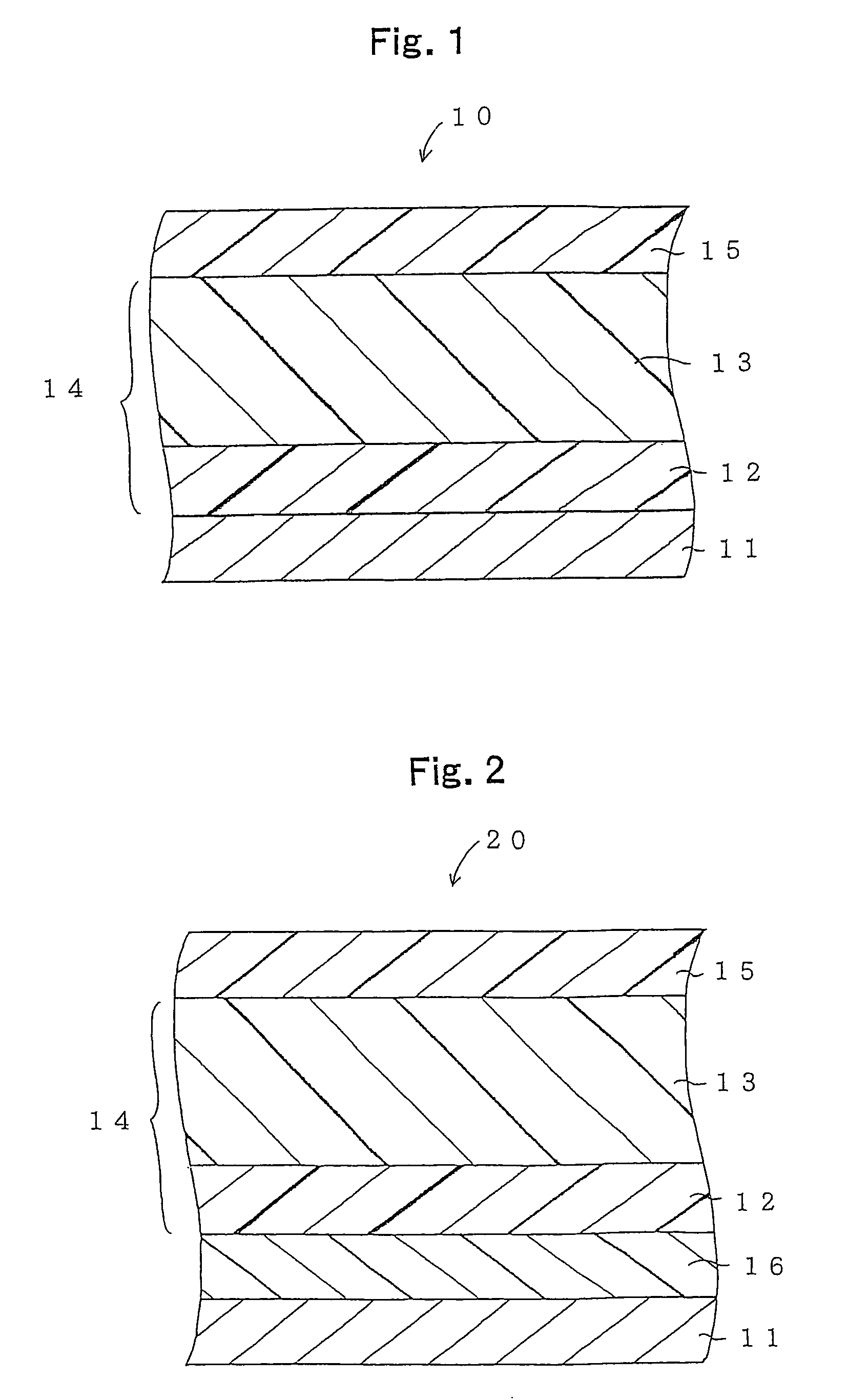
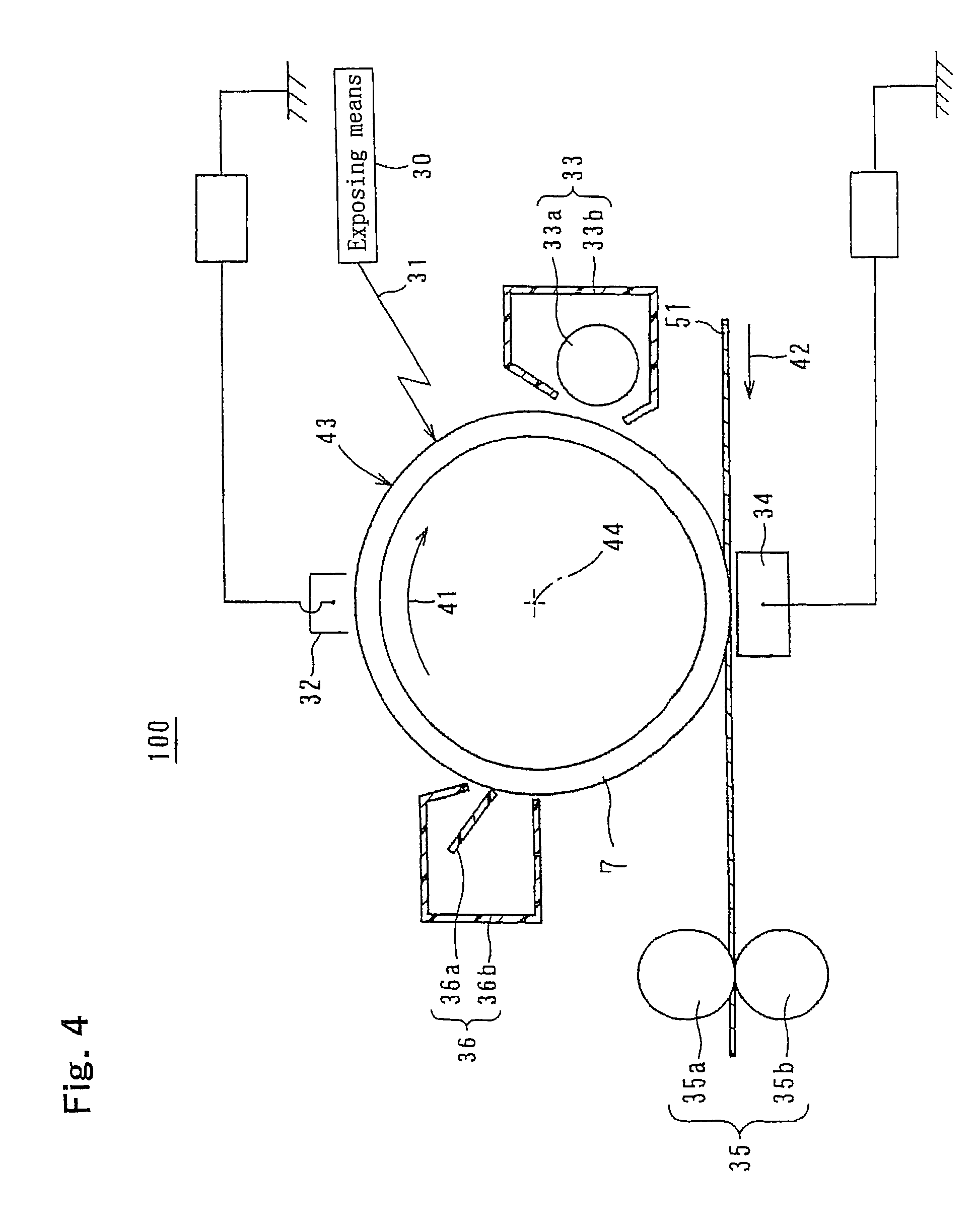
[0080]FIG. 1 is a partially sectional view showing the simplified structure of an embodiment 1 of the electrophotographic photoconductor of the present invention. This electrophotographic photoconductor 10 has a cylindrical form and is used in an image forming apparatus 100 as shown in FIG. 4. The image forming apparatus provided with the photoconductor 10 of the present invention will be explained in detail wherein the symbol 7 represents the photoconductor in FIG. 4.

[0081]As shown in FIG. 1, this photoconductor 10 has a cylindrical conductive support 11 made of an conductive material, a charge generation layer 12 which is a layer laminated on the conductive support 11 and contains a charge generation material, a charge transport layer 13 which is a layer laminated on the charge generation layer 12 and contains a charge transport material and a surface protective layer 15 which is a layer laminated on the charge transport layer 13 and contains the amine compound of the formula (1)....

embodiment 2

[0125]FIG. 2 is a partial sectional view simply showing the structure of an embodiment 2 of the electrophotographic photoconductor of the present invention. The electrophotographic photoconductor 20 of the embodiment 2 is different from the electrophotographic photoconductor 10 of the embodiment 1 in the point that an intermediate layer 16 is disposed between the conductive support 11 and the light-sensitive layer (laminate type photoconductive layer) 14. Other structures in this embodiment 2 are the same as those in the embodiment 1. Therefore, the same elements are represented by the same symbols and the explanations of these elements are not repeated here.

[0126]The role of the intermediate layer 16 will be explained.

[0127]In the case where the intermediate layer 16 is not formed between the conductive support 11 and the light-sensitive layer 14, there is the case where charges are injected into the light-sensitive layer 14 from the conductive support 11, the electrostatic propert...

embodiment 3

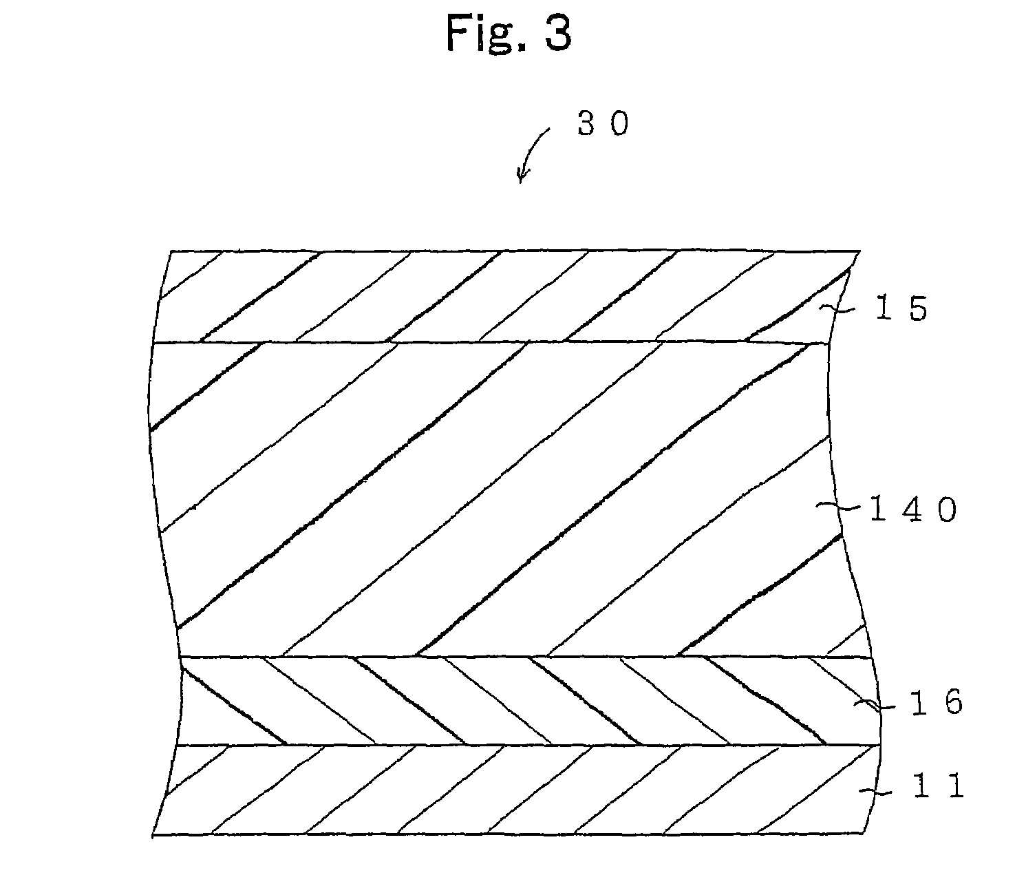
[0137]FIG. 3 is a partial sectional view simply showing the structure of an embodiment 3 of the electrophotographic photoconductor of the present invention. The electrophotographic photoconductor 30 of the embodiment 3 is different from the electrophotographic photoconductor 20 of the embodiment 2 in the point that a light-sensitive layer (single layer type photoconductive layer) 140 having a single layer containing both the charge generation material and the charge transport material is disposed on the intermediate layer 16. Other structures in this embodiment 3 are the same as those in the embodiment 2. Therefore, the same elements are represented by the same symbols and the explanations of these elements are not repeated here.

[0138]The single layer type photoconductor 30 of this embodiment 3 is suitable for a photoconductor for a positive charge type image forming apparatus reduced in the generation of ozone. Also, because the light-sensitive layer 140 is a single layer in the si...


PUM


Abstract

An electrophotographic photoconductor of the invention comprising: an conductive support; a light-sensitive layer formed on the conductive support and containing a charge generating material and a charge transport material; and a surface protective layer formed on the light-sensitive layer and made of a resin composition, wherein the resin composition constituting the surface protective layer contains an amine compound represented by the following formula (1):wherein R1 and R2 are, the same or different, each an alkyl group or an allyl group which may have a substituent or a heterocyclic residue to be formed through or not through a nitrogen atom or an oxygen atom together with the nitrogen atom to which R1 and R2 are bonded, R3 and R4 are, the same or different, each an alkyl group having a substituent and n denotes 1 or 2, provided that when n is 1, X is a hydrogen atom, a halogen atom, or an alkyl group, a hydroxyl group or a mercapto group which may have a substituent, or a ring optionally containing an oxygen atom and a nitrogen atom between carbon atoms and when n is 2, X is an oxygen atom or a sulfur atom.

Description

CROSS-REFERENCE TO RELATED APPLICATION[0001]This application is related to Japanese patent application No. 2006-005018 filed on Jan. 12, 2006 whose priority is claimed under 35 USC §119, the disclosure of which is incorporated by reference in its entirety.BACKGROUND OF THE INVENTION[0002]1. Field of the Invention[0003]The invention relates to an electrophotographic photoconductor to be used for image formation by an electrophotographic system, a method of producing the electrophotographic photoconductor and an image forming apparatus using the electrophotographic-photoconductor.[0004]2. Description of the Related Art[0005]Electrophotographic photoconductors which are used to form an image in an electrophotographic system and exposed to light corresponding to image information to thereby form an electrostatic latent image are used in image forming apparatuses. These image forming apparatuses provided with this electrophotographic photoconductor are widely utilized not only in copying...

Claims


Application Information

Patent Timeline
Patent Type & Authority Patents(United States)
IPC IPC(8): G03G5/14
CPCG03G5/0614G03G5/14708G03G5/14734
Inventor SUGIMURA, HIROSHIFUKUSHIMA, KOTAROTORIYAMA, KOICHI
Owner SHARP KK
Why Eureka
Try Eureka