Source driver, method for manufacturing same, and liquid crystal module

a source driver and liquid crystal module technology, applied in non-linear optics, instruments, optics, etc., can solve the problems of increasing heat generation of semiconductor chips b>514/b>, and achieve the effect of reducing the total cost of the liquid crystal module, reducing the cost of the source driver, and improving heat dissipation properties

Active Publication Date: 2013-02-12
SHENZHEN TOREY MICROELECTRONIC TECH CO LTD
View PDF15 Cites 0 Cited by
  • Summary
  • Abstract
  • Description
  • Claims
  • Application Information

AI Technical Summary

Benefits of technology

[0014]In recent years, a TV has been developed to have high functions and multi-outputs. Such developments cause an increase in heat generation by the semiconductor chip 514 provided on the source driver 503. Because of such an increase, the heat generation by the semiconductor chip 514 is becoming a more serious problem than before. For this reason, there has been demand for a source driver which can dissipate the heat more efficiently.

Problems solved by technology

Because of such an increase, the heat generation by the semiconductor chip 514 is becoming a more serious problem than before.

Method used


Image

  • Source driver, method for manufacturing same, and liquid crystal module
  • Source driver, method for manufacturing same, and liquid crystal module
  • Source driver, method for manufacturing same, and liquid crystal module

Examples


embodiment 1

Arrangement of Source Driver

[0078]One embodiment of the present invention is described below with reference to drawings.

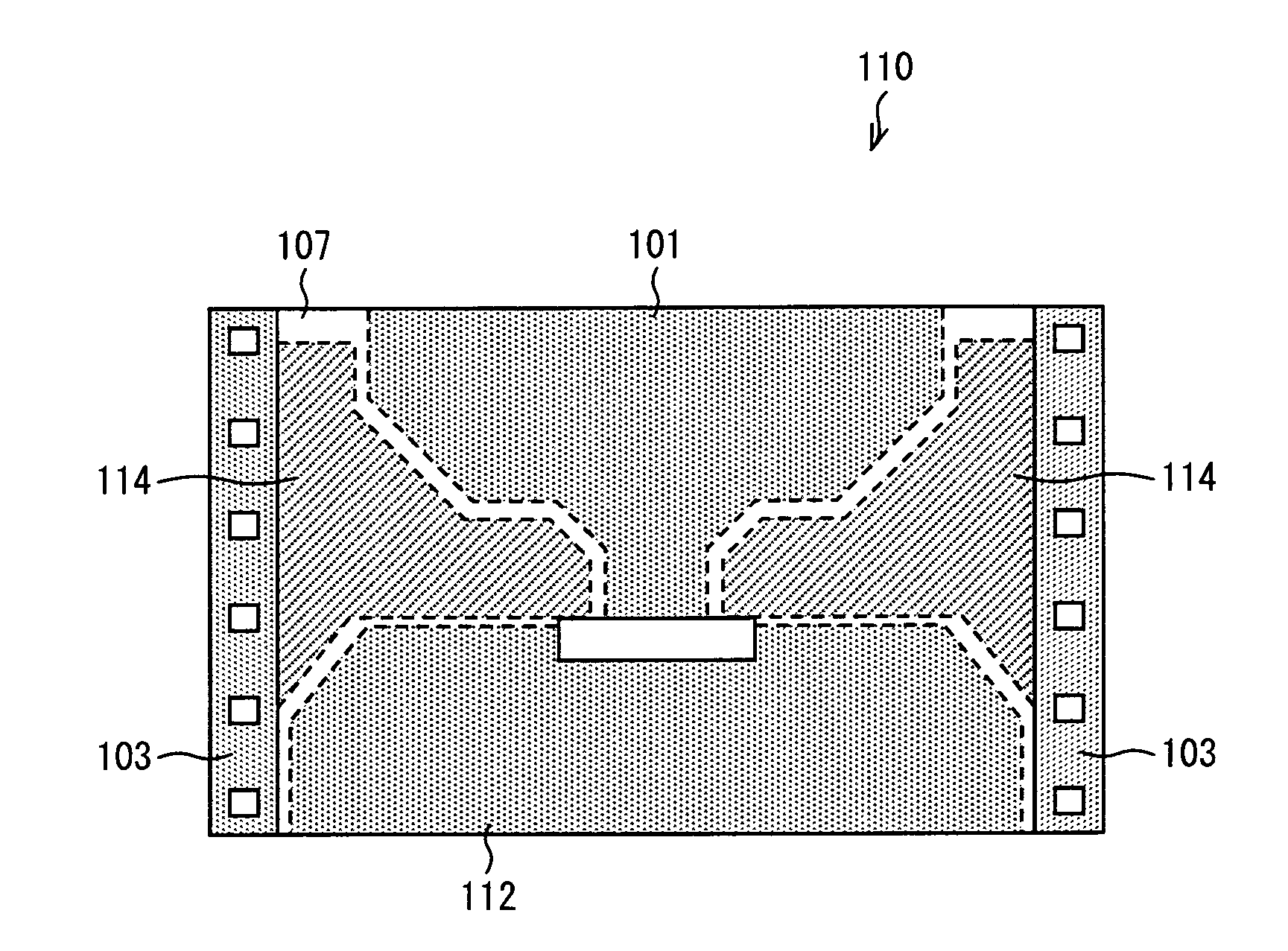
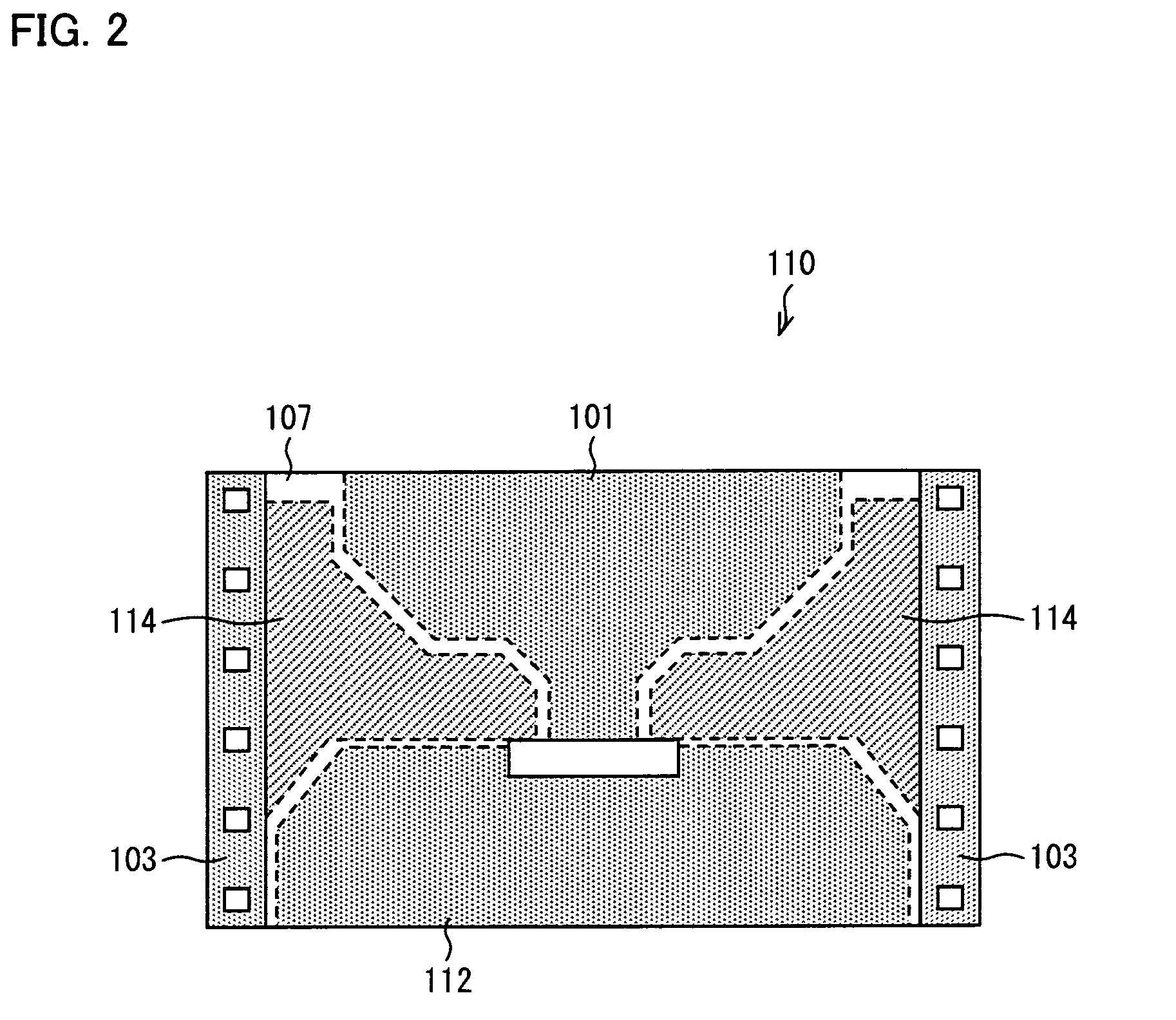
[0079]FIG. 1 is a view illustrating an example of an arrangement of a source driver 100 of the present embodiment.

[0080]The source driver 100 of the present embodiment includes a film substrate 107 as a base. An input terminal wiring region 101, an output terminal wiring region 102, and two heat conducting patterns 104 (third wiring line) are provided on the film substrate 107. The source driver 100 includes a semiconductor chip 105 on the film substrate 107. The film substrate 107 has two sprocket portions 103. The sprocket portions 103 are provided at opposite ends of the film substrate 107, respectively. That is, the source driver 100 is a semiconductor device of a film package type.

[0081]The input terminal wiring region 101 is a region in which wiring lines (first wiring lines) (not illustrated) are provided. The first wiring lines are connected to input termin...

embodiment 2

[0105]Another embodiment of the present invention is described below with reference to drawings. Note that an arrangement of the present embodiment is the same as the arrangement of Embodiment 1 except arrangements described below. Further, members having the same functions as those of the members illustrated in the drawings referenced in Embodiment 1 have the same signs, and explanations of these are omitted, for the sake of simple explanation.

[0106]FIG. 4 is a cross-sectional side view illustrating an example of an arrangement of a source driver 200 of the present embodiment.

[0107]The source driver 200 of the present embodiment is such that the source driver 100 of Embodiment 1 further includes a heat dissipating material 201 attached to an upper surface of a semiconductor chip 105 with the use of an adhesive agent 203, which heat dissipating material 201 has suspender leads 202 (see FIG. 4).

[0108]The heat dissipating material 201 is a metal plate (heat spreader), and may be selec...

embodiment 3

[0113]Further another embodiment of the present invention is described below with reference to drawings. Note that an arrangement of the present embodiment is the same as the arrangements of Embodiments 1 and 2, except arrangements described below. Further, members having the same functions as those of the members illustrated in the drawings referenced in Embodiments 1 and 2 have the same signs, and explanations of these are omitted, for the sake of simple explanation.

[0114]FIG. 5 is a view illustrating an example of an arrangement of a liquid crystal module 300 of the present embodiment.

[0115]The liquid crystal module 300 of the present embodiment includes a liquid crystal panel 301, gate drivers 302, wiring tapes 303, input substrates 304, and source drivers 100 of Embodiment 1 (see FIG. 5). To one of four sides of the liquid crystal panel 301, 10 source drivers 100 are attached, and 3 gate drivers 302 are attached to each of opposite two sides of the four sides, which two sides a...


PUM


Abstract

A source driver of a film package type including a film substrate; a semiconductor chip on a surface of the film substrate, the semiconductor chip having a plurality of terminals, the plurality of terminals including input terminals, output terminals, and third terminals; an input terminal wiring region for receiving first wiring lines which are connected to the input terminals; an output terminal wiring region for receiving second wiring lines which are connected to the output terminals; sprocket portions at opposite ends of the film substrate; and a heat conducting patterns for connecting the third terminals. This makes it possible to provide a source driver, a method for manufacturing the source driver, and a liquid crystal module, each of which can increase a heat dissipation amount.

Description

TECHNICAL FIELD[0001]The present invention relates to a source driver of a film package type, a method for manufacturing the source driver, and a liquid crystal module including the source driver.BACKGROUND ART[0002]A package in which a semiconductor chip is provided on an insulating film on which a wiring pattern is formed, such as a TCP (Tape Carrier Package) or a COF (Chip on Film), is widely used as a package for an LCD driver which is attached to a liquid crystal panel or the like. Examples of the LCD driver encompass: a source driver for supplying a signal to a source electrode of a transistor provided in a pixel region in a liquid crystal panel; and a gate driver for supplying a signal to a gate electrode of the transistor.[0003]FIG. 7 is a view schematically illustrating an arrangement of a conventional liquid crystal module 500.[0004]The conventional liquid crystal module 500 includes a liquid crystal panel 501, gate drivers 502, source drivers 503, and input substrates 504...

Claims


Application Information

Patent Timeline
Patent Type & Authority Patents(United States)
IPC IPC(8): H01L23/48
CPCH01L23/4985H01L24/97H05K1/0209H01L23/49568H01L24/13H01L24/16H01L24/32H01L24/81H01L2224/73253H01L2224/81203H01L2224/81801H01L2224/97H01L2924/01029H01L2924/01033H01L2924/01078H01L2924/01079H01L2924/01082H01L2924/01322H01L2924/19041H01L2924/19107H05K1/189H05K3/361H05K2201/09781H05K2201/10681H01L2924/01005H01L2924/01006H01L2924/01023H01L2924/12041H01L2224/73204
Inventor KATOH, TATSUYA
Owner SHENZHEN TOREY MICROELECTRONIC TECH CO LTD
Why Eureka
Try Eureka