Method and apparatus of growing silicon single crystal and silicon wafer fabricated thereby

a technology of silicon single crystal and fabricated silicon wafers, which is applied in the direction of crystal growth process polycrystalline material growth, etc., can solve the problems of poor device yield, micro precipitates formed from point defects, and insufficient control of single crystal temperature gradients, etc., to eliminate faults in actual fabrication of devices.

Active Publication Date: 2006-06-29
LG SILTRON
View PDF2 Cites 9 Cited by
  • Summary
  • Abstract
  • Description
  • Claims
  • Application Information

AI Technical Summary

Benefits of technology

[0018] The present invention has been made to solve the foregoing problems of the prior art and it is therefore an object of the present invention to provide a method and apparatus fo

Problems solved by technology

However, controlling the temperature gradient of single crystal is, by itself, not sufficient to manufacture a high quality Si single crystal ingot and a Si wafer having low point defect concentration.
In particular, in case of fabricating semiconductor devices from a Si wafer manufactured according to a conventional technique, micro precipitates are formed from point defects through repeated heat treatment in device fabrication.
As a drawback, the micro precipitates cause faults, resulting in poor device yield.
Unless sufficient out-diffusion takes place in vicinity to the wafer, interstitial crystal defects such as LDP occur.
However, these conventional techniques are based upon solid state reaction, and thus have the following problems: First, there are a number of hindr

Method used


Image

  • Method and apparatus of growing silicon single crystal and silicon wafer fabricated thereby
  • Method and apparatus of growing silicon single crystal and silicon wafer fabricated thereby
  • Method and apparatus of growing silicon single crystal and silicon wafer fabricated thereby

Examples


Embodiment Construction

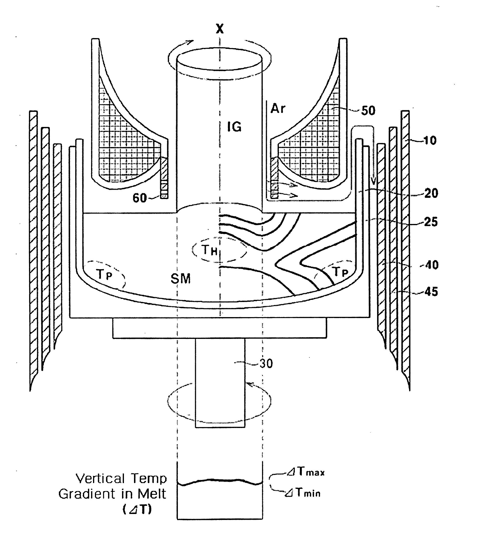
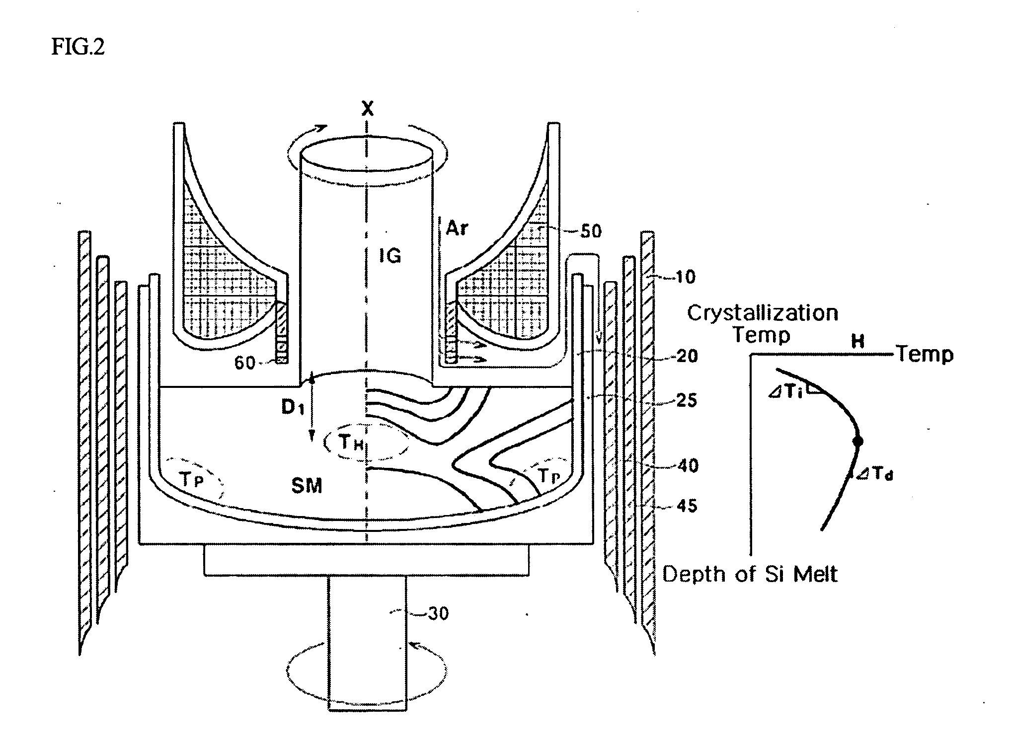
[0047] Hereinafter, a preferred embodiment of the present invention will be described with reference to the accompanying drawings. In the following description and drawings, the same reference numerals are used to designate the same or similar components, and so repetition of the description on the same or similar components will be omitted.

[0048] The present invention starts from the conception that in growing solid Si single crystal from Si melt, the growth of a high quality Si single crystal ingot with minimized point defect is not obtained from merely controlling single crystal temperature gradient and solid-liquid interface profile, and is made based upon the fact that there exists a more decisive factor for the growth of a high quality Si single crystal.

[0049] In order to overcome restrictions in solid state reaction occurring in subsequent to crystallization, liquid state prior to solidification has been analyzed thoroughly, and as a result, it was found that the temperatur...


PUM


Abstract

Disclosed is a metod of fabrication of high quality silicon single crystal at high growth rate. The method grows silicon single crystal from silicon melt by Czochralski method, wherein the silicon single crystal is grown according to conditions that the silicon melt has an axial temperature gradient determined according to an equation, {(ΔTmax−ΔTmin)/ΔTmin}×100≦10, wherein ΔTmax is a maximum axial temperature gradient of the silicon melt and ΔTmin is a minimum axial temperature gradient of the silicon melt, when the axial temperature gradient is measured along an axis parallel to a radial direction of the silicon single crystal.

Description

BACKGROUND OF THE INVENTION [0001] 1. Field of the Invention [0002] The present invention relates to a method of growing high quality silicon single crystal, and more particularly, to a method and apparatus of growing a high quality silicon single crystal ingot by controlling temperature distribution of silicon melt during Czochralski growth of silicon single crystal, and silicone wafer fabricated thereby. [0003] 2. Description of the Related Art [0004] As well known in the art, in order to grow a high quality silicon (Si) single crystal ingot that can enhance semiconductor device yield, temperature control has been conducted on high temperature distribution of the single crystal ingot mainly after crystallization. This methodology is intended to control stress that may be induced from contraction owing to cooling subsequent to crystallization or by the behavior of point defects built up in solidification. [0005] According to a typical process of Czochralski growth of Si single crys...

Claims


Application Information

Patent Timeline
IPC IPC(8): C30B15/00C30B21/06C30B13/00C30B27/02C30B21/04C30B28/08C30B28/10C30B30/04
CPCC30B15/00C30B15/14C30B15/20Y10T117/1088C30B29/06Y10S117/917Y10T117/1068C30B15/203
Inventor CHO, HYON-JONG
Owner LG SILTRON
Why Eureka
Try Eureka