Final passivation scheme for integrated circuits

a passivation scheme and integrated circuit technology, applied in the direction of electrical apparatus, semiconductor devices, semiconductor/solid-state device details, etc., can solve the problems of cracks in the passivation layers damage to the al pads and the underlying rigid passivation layer, and inability to crack the passivation layer below the probing area, so as to protect against crack related reliability failures and high resistance to crack propagation

Active Publication Date: 2005-11-24
INFINEON TECH AG
View PDF8 Cites 18 Cited by
  • Summary
  • Abstract
  • Description
  • Claims
  • Application Information

AI Technical Summary

Benefits of technology

[0018] The introduction of the buffer layer using a dielectric material with a lower modules material and with high resistance to crack propagation (e.g. SiLK™, a product of Dow Ch

Problems solved by technology

Current probing/testing operations at wafer level are known to induce cracks in the passivation layers below the probing area due to the mechanical forces applied by the probing process.
These cracks can propagate into the chip and cause corrosion of the interconnects (e.g., copper wiring) resulting in reliability failures.
For example, the probing process using conventional probe techniques (e.g., cantilever—vertical—membrane, etc.) can cause damage on the Al pads and the underlying rigid passivation layer (mo

Method used


Image

  • Final passivation scheme for integrated circuits
  • Final passivation scheme for integrated circuits
  • Final passivation scheme for integrated circuits

Examples


first embodiment

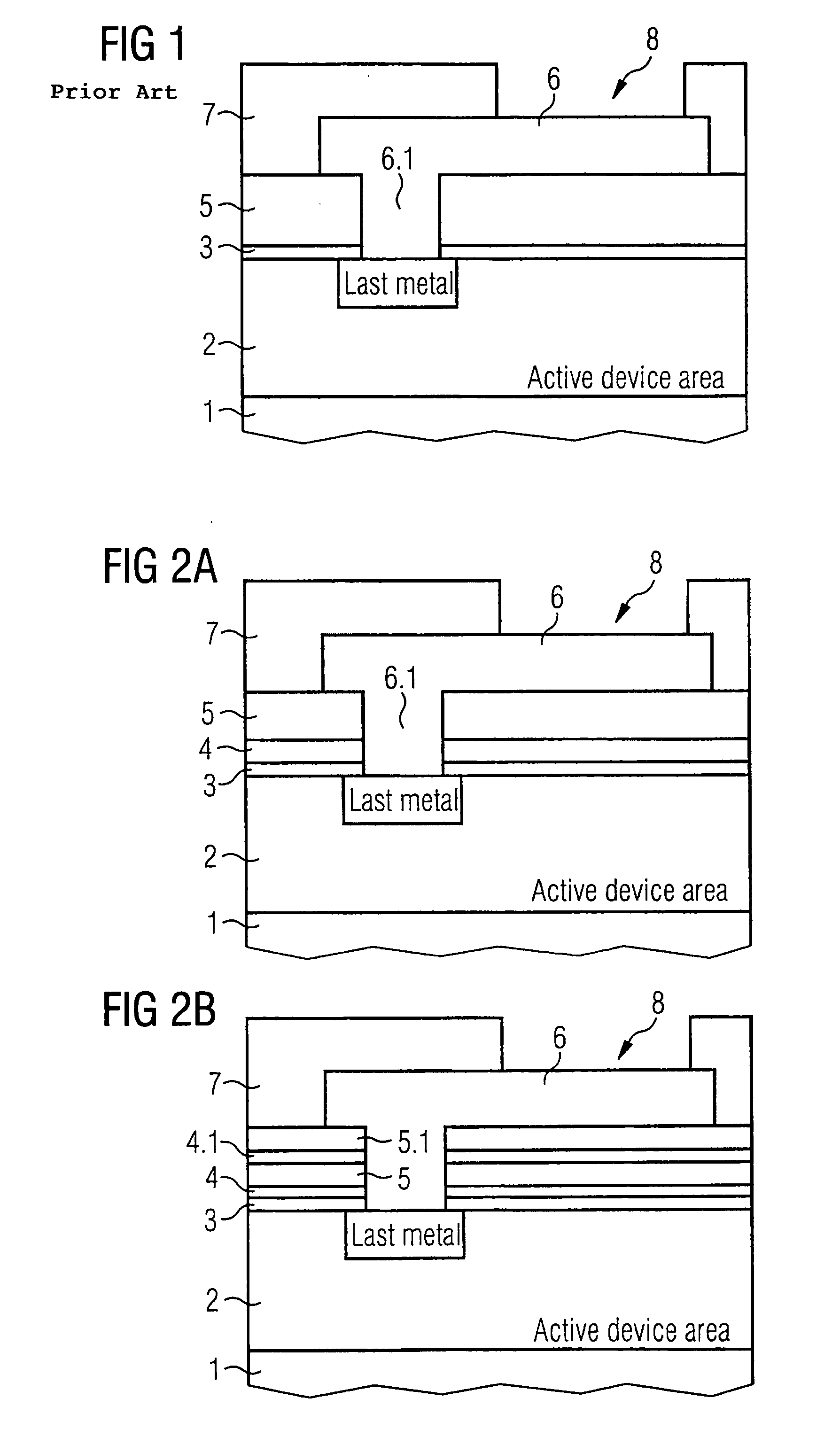
[0028]FIG. 2, which includes FIGS. 2A and 2B, and FIG. 3, which includes FIGS. 3A-3D, show the invention with the novel final passivation scheme. This scheme provides for highly reliable final probing.

[0029] The device of FIGS. 2 and 3 includes a wafer or substrate 1 that is preferably formed from silicon, although other semiconductors such as silicon germanium or gallium arsenide can be used. The device and interconnect layers are collectively referred to as the active device area and labeled with reference numeral 2. This region includes the active devices (e.g., transistors), passive devices (e.g., capacitors, resistors), and any interconnects (e.g., multilevel copper damascene). The last level interconnect capping layer 3 is explicitly shown. The capping layer 3 commonly comprises SiN (e.g., Si3N4) with a thickness between about 50 to about 200 nm. Other capping layers such as SiO2 and SiON can also be used.

[0030] A buffer layer / crack stop layer 4 is deposited over the capping ...

second embodiment

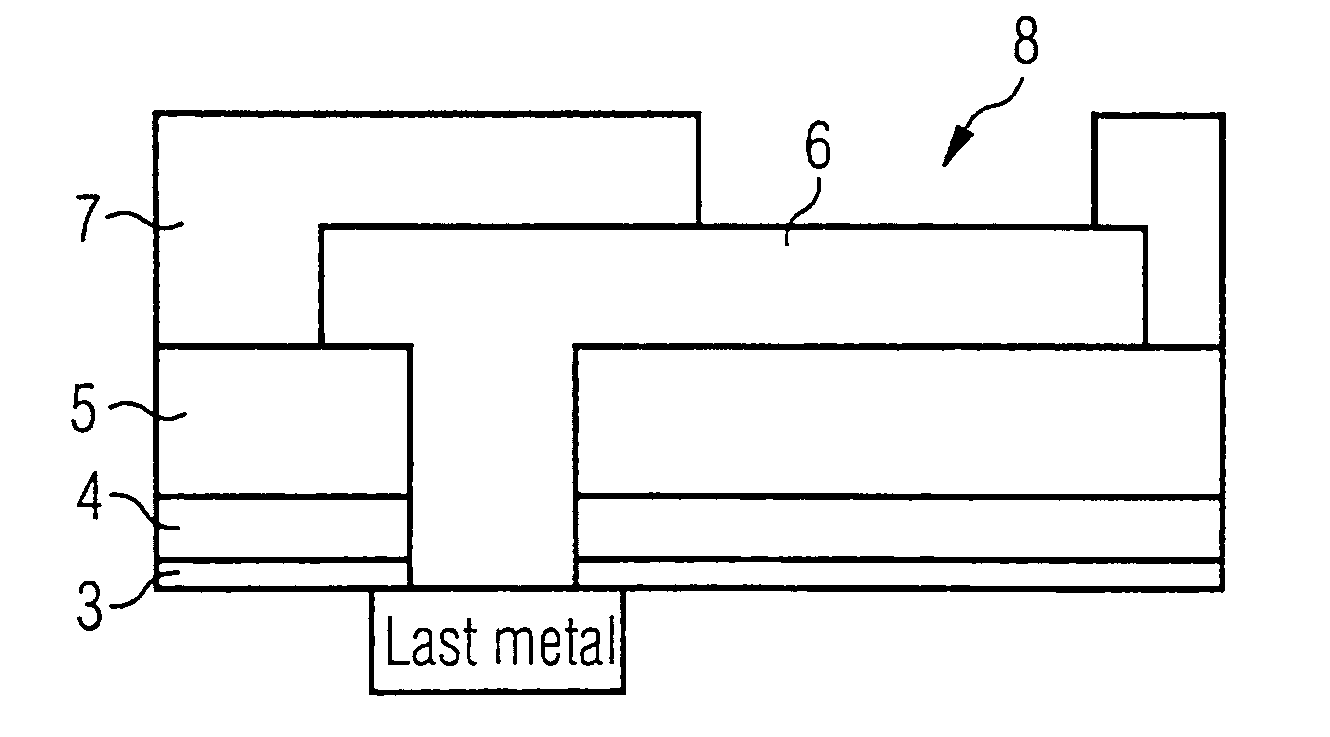
[0034]FIG. 2B shows the invention with multiple buffer layers / crack stop layers 4, 4.1 and passivation layer 5, 5.1 between the last upper metal in the device and interconnect layers 2 divided by a last level interconnect capping layer 3 and an aluminum probe / wire bond / flip-chip pad 6.

[0035] The Al probe / wire bond / flip-chip pad 6 is connected over a via 6.1 through the passivation layer 5, 5.1, through the buffer layer / crack stop layer 4, 4.1 and through the last level interconnect capping layer 3 with the last metal of the device and interconnect layers 2.

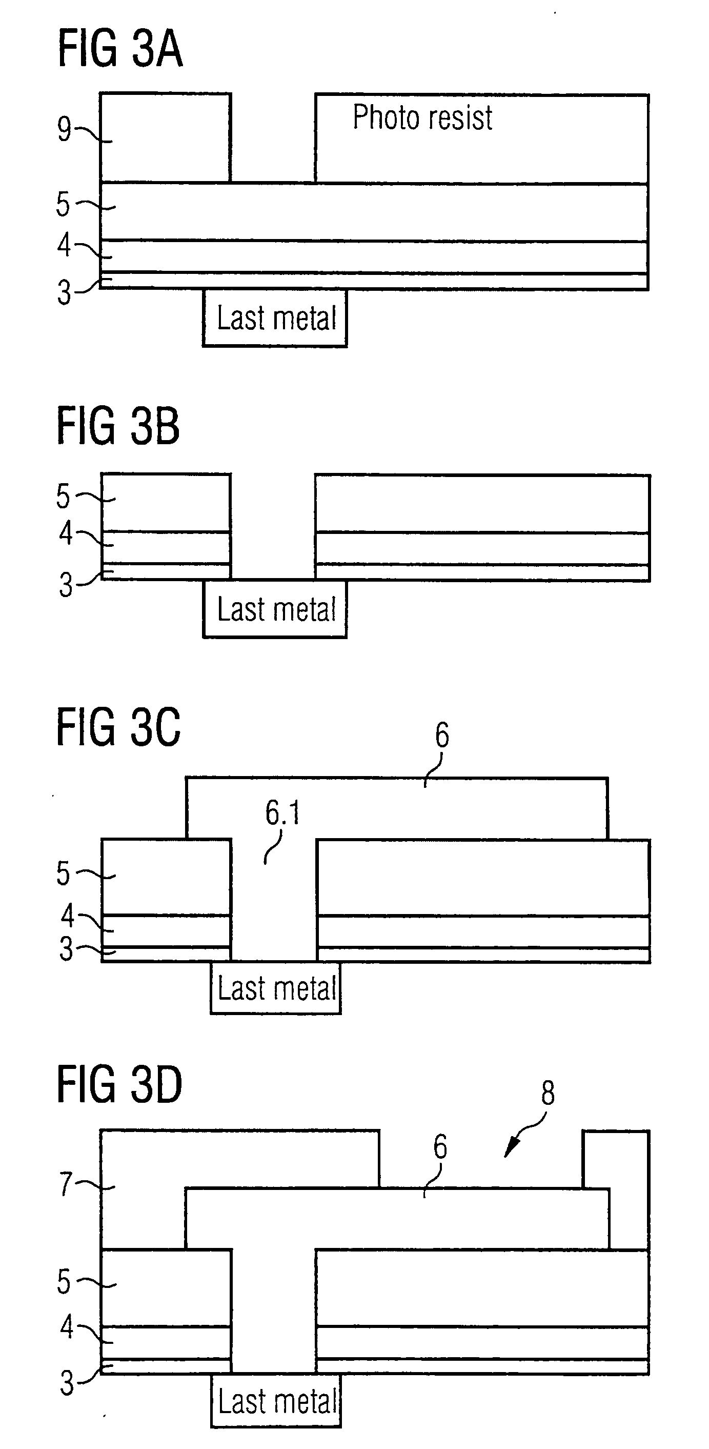
[0036]FIGS. 3A-3D illustrate a sequence showing the steps to realize such a buffer layer / crack stop layer 4 below the aluminum probe / wire bond / flip-chip pad 6.

[0037]FIG. 3A presents the last metal in the device and interconnect capping layer 3 covered by a last level interconnect cap layer 3, e.g., a 70 nm SiN cap layer. Over this cap layer is deposited a 200 nm SiLK™ buffer layer 4 by spin-on and cure and over this layer a pass...


PUM


Abstract

A semiconductor device includes a substrate with an active area. A last level interconnect capping layer is disposed over the active area. A buffer layer/crack stop layer overlies the last level interconnect capping layer and a passivation layer overlies the buffer layer/crack stop layer. Also, a contact pad (e.g., probe pad, wire bond pad or flip-chip pad) overlies the passivation layer.

Description

TECHNICAL FIELD [0001] The present invention relates generally to integrated circuits, and more particularly to a final passivation scheme for integrated circuits. BACKGROUND [0002] It is known and necessary that finally produced integrated circuits (chips) must be tested in the wafer compound to find out the good dies. Such a test is performed with so-called wafer prober equipments that have needle cards or similar contacting elements, which are used to realize an electrical contact between the tips of the needles or the other contacting elements and contact pads made of aluminum or another metal on the wafer. [0003] As soon as the electrical contact is realized, the wafer prober generates test sequences for testing the integrated circuit. To realize a good electrical contact between the tips of the needles of the needle card and the Al pads it is necessary to generate a contact with sufficient force between the contact partners so that the result is a good electrical contact. [000...

Claims


Application Information

Patent Timeline
IPC IPC(8): H01L21/31H01L21/312H01L21/314H01L21/44H01L21/469H01L21/768H01L23/31
CPCH01L21/312H01L21/3144H01L21/76801H01L21/76829H01L23/3171H01L2924/0002H01L23/3192H01L2924/19041H01L2924/00H01L21/02304H01L21/02118H01L21/022
Inventor KALTALIOGLU, ERDEMPILS, CHRISTIAN
Owner INFINEON TECH AG
Why Eureka
Try Eureka