Stacked DIMM memory interface

a memory interface and dimming technology, applied in the field of memory subsystems, can solve the problems of limiting the increase in bandwidth, introducing significant latency, and limiting the intra-device command scheduling constraints, and achieve the effect of high memory performan

Active Publication Date: 2013-02-26
GOOGLE LLC
View PDF839 Cites 33 Cited by
  • Summary
  • Abstract
  • Description
  • Claims
  • Application Information

AI Technical Summary

Benefits of technology

[0014]One advantage of the disclosed interface circuit is that it can provide higher memory performance by not requiring idle bus cycles to turnaround the data bus when switching from reading from one memory device to reading from another memory device, or from writing to one memory device to writing to another memory device.

Problems solved by technology

However, command scheduling constraints that exist in the memory systems limit the command issue rates, and consequently, limit the increase in bandwidth.
The intra-device command-scheduling constraints typically arise because parts of the memory device (e.g. column, row, bank, etc.) share a resource inside the memory device.
However, there are several problems associated with such an approach.
One problem is that the FBDIMM approach introduces significant latency (see description, below).
Another problem is that the FBDIMM approach requires a specialized memory controller capable of processing the assembly.
As memory speed increases, the introduction of latency becomes more and more of a detriment to the operation of the memory system.
Even modern FBDIMM-type memory systems introduce 10 s of nanoseconds of delay as the packet is assembled.
Moreover, the implementation of the FBDIMM-type memory devices required corresponding changes in the behavior of the memory controller, and this FBDIMMS are not backward compatible among industry-standard memory system.

Method used


Image

  • Stacked DIMM memory interface
  • Stacked DIMM memory interface
  • Stacked DIMM memory interface

Examples


Embodiment Construction

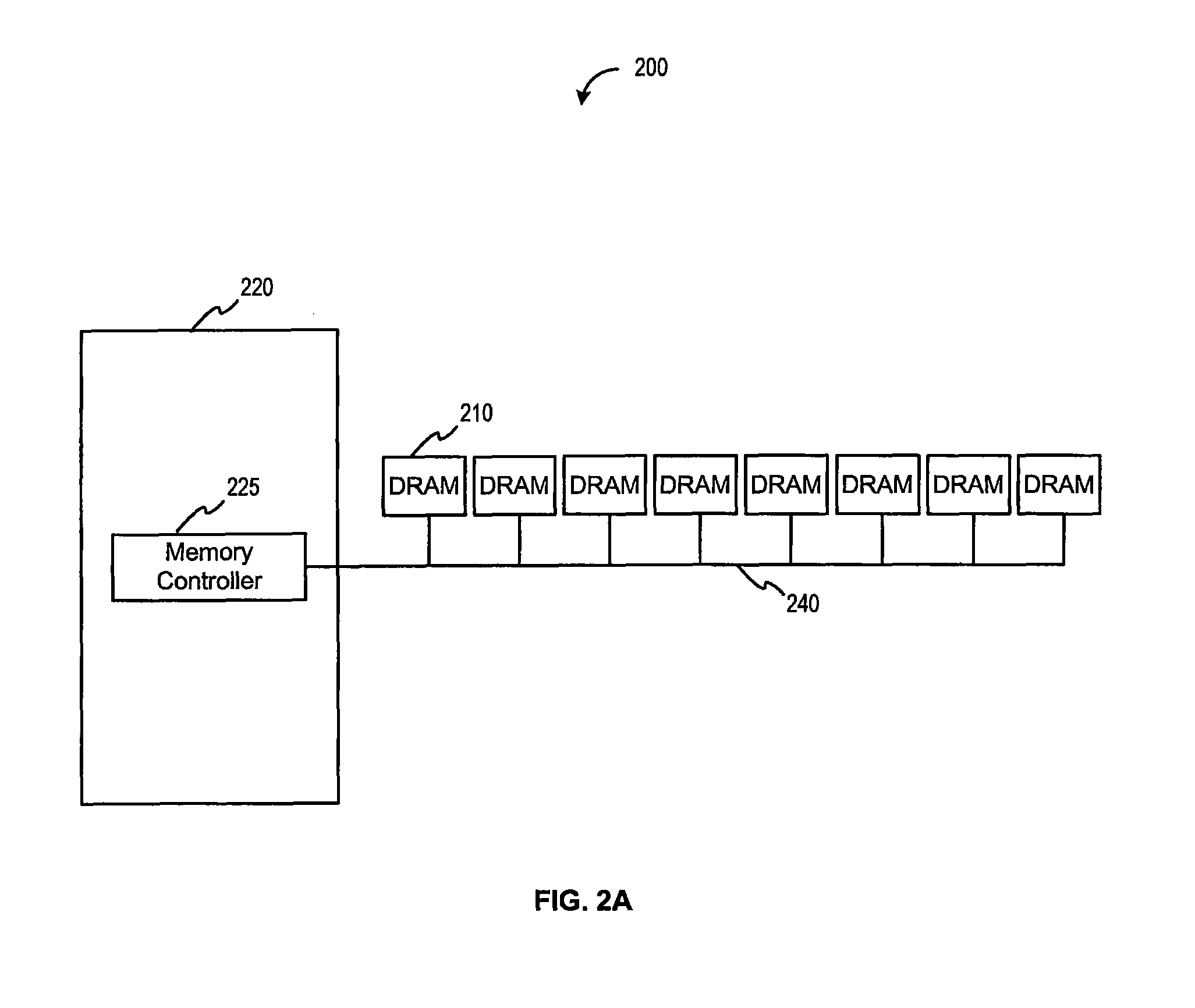
[0028]FIG. 2A illustrates major logical components of a computer platform 200, according to prior art. As shown, the computer platform 200 includes a system 220 and an array of memory components 210 interconnected via a parallel interface bus 240. As also shown, the system 220 further includes a memory controller 225.

[0029]FIG. 2B illustrates major logical components of a computer platform 201, according to one embodiment of the present invention. As shown, the computer platform 201 includes the system 220 (e.g., a processing unit) that further includes the memory controller 225. The computer platform 201 also includes an array of memory components 210 interconnected to an interface circuit 250, which is connected to the system 220 via the parallel interface bus 240. In various embodiments, the memory components 210 may include logical or physical components. In one embodiment, the memory components 210 may include DRAM devices. In such a case, commands from the memory controller 22...


PUM


Abstract

One embodiment of the present invention sets forth an interface circuit configured to combine time staggered data bursts returned by multiple memory devices into a larger contiguous data burst. As a result, an accurate timing reference for data transmission that retains the use of data (DQ) and data strobe (DQS) signals in an infrastructure-compatible system while eliminating the cost of the idle cycles required for data bus turnarounds to switch from reading from one memory device to reading from another memory device, or from writing to one memory device to writing to another memory device may be obtained, thereby increasing memory system bandwidth relative to the prior art approaches.

Description

BACKGROUND OF THE INVENTION[0001]1. Field of the Invention[0002]Embodiments of the present invention generally relate to memory subsystems and, more specifically, to improvements to such memory subsystems.[0003]2. Description of the Related Art[0004]Memory circuit speeds remain relatively constant, but the required data transfer speeds and bandwidth of memory systems are increasing, currently doubling every three years. The result is that more commands must be scheduled, issued and pipelined in a memory system to increase bandwidth. However, command scheduling constraints that exist in the memory systems limit the command issue rates, and consequently, limit the increase in bandwidth.[0005]In general, there are two classes of command scheduling constraints that limit command scheduling and command issue rates in memory systems: inter-device command scheduling constraints, and intra-device command scheduling constraints. These command scheduling constraints and other timing constrain...

Claims


Application Information

Patent Timeline
Patent Type & Authority Patents(United States)
IPC IPC(8): G06F13/28
CPCG06F13/28G11C7/22G06F13/1689G06F1/12
Inventor WANG, DAVID T.RAJAN, SURESH NATARAJAN
Owner GOOGLE LLC
Why Eureka
Try Eureka