Wideband I-V probe and method
a technology of i-v probes and probes, applied in the direction of resistance/reactance/impedence, instruments, measurement devices, etc., can solve the problems of limiting the frequency bandwidth, assembly cannot be considered, and the phase offset cannot be desired
- Summary
- Abstract
- Description
- Claims
- Application Information
AI Technical Summary
Benefits of technology
Problems solved by technology
Method used
Image
Examples
Embodiment Construction
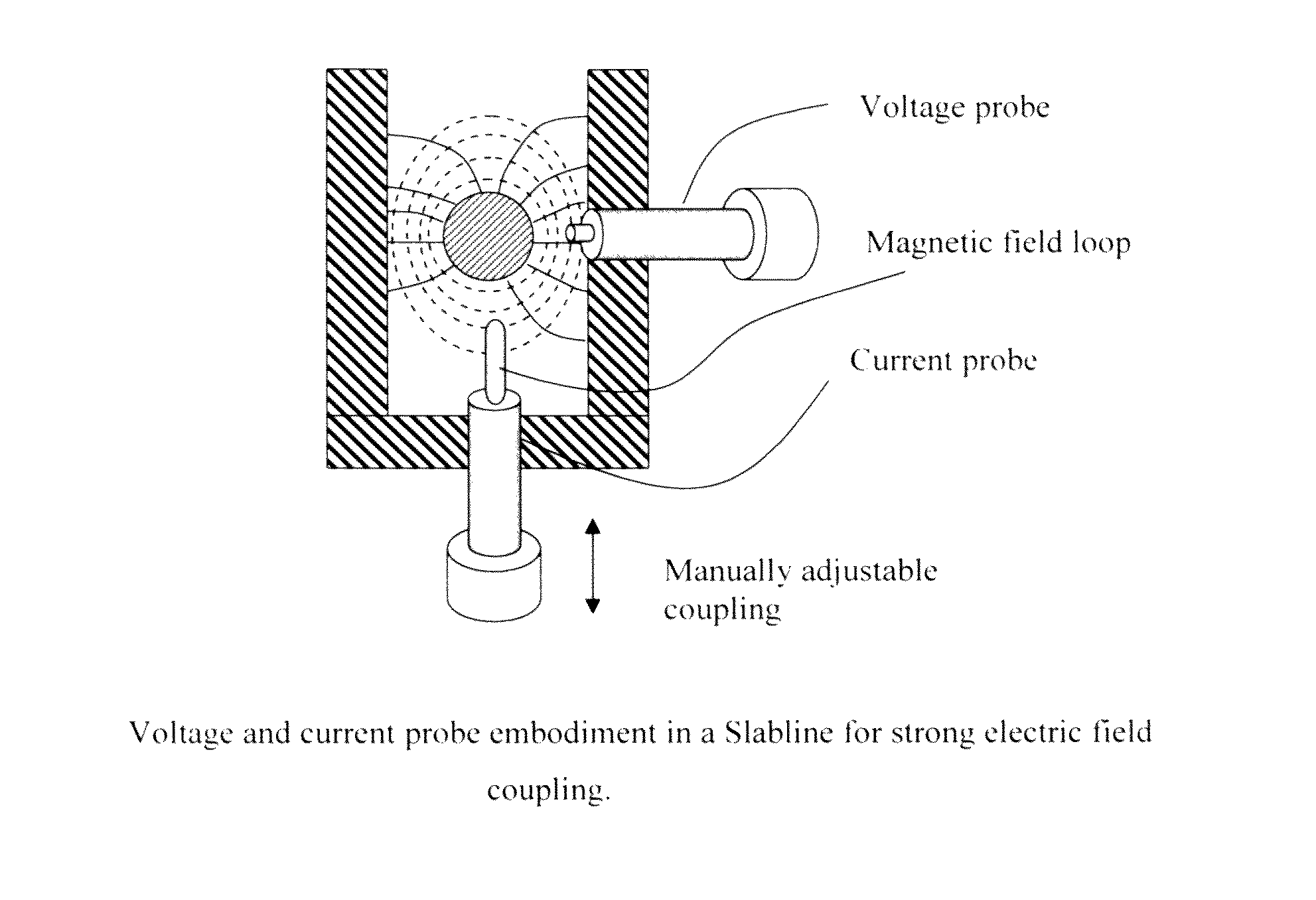
[0052]The electric-magnetic field sensor assembly described here avoids the shortcomings of existing solutions; the fact that said sensor assembly is mounted inside a low loss slabline (FIG. 11) allows an orthogonal configuration, in which the electric field sensor is close to the strongest area of the electric field and the magnetic field sensor is shielded by the center conductor and detects the magnetic field either at the bottom or at the top of said slabline, in which area the electric field is weakest and least disturbed.
[0053]Even though there will be a small electric field deformation due to the presence of said magnetic field loop at the bottom of said slabline, the electric field in this area is quasi zero, because in the slabline structure the electric field is concentrated towards the sidewalls (FIG. 10). The magnetic to electric field influence is therefore the smallest possible.
[0054]The electric current, induced into the electric field sensor creates a surrounding mag...
PUM
 Abstract
Description
Claims
Application Information


