Wireless IC device component and wireless IC device

a technology of integrated circuits and components, applied in loop antennas, resonant antennas, instruments, etc., can solve the problems of increasing the value of inductive reactance, long electrical length, etc., and achieve the effect of improving the radiation characteristics of signals, reducing the frequency band, and efficiently transmitting

Active Publication Date: 2013-04-16
MURATA MFG CO LTD
View PDF488 Cites 7 Cited by
  • Summary
  • Abstract
  • Description
  • Claims
  • Application Information

AI Technical Summary

Benefits of technology

[0007]To overcome the problems described above, preferred embodiments of the present invention provide a wireless IC device component and a wireless IC device that are capable of increasing the electrical length of a coupling electrode and achieving satisfactory impedance matching between a wireless IC and a radiation plate to more satisfactorily couple the coupling electrode to the radiation plate.
[0011]In the wireless IC device component of the first preferred embodiment and the wireless IC device of the second preferred embodiment, the coupling electrode is preferably defined by an annular electrode via the pair of ends that are capacitively coupled to each other. The coupling electrode has an inductive reactance (XL: jωL) caused by the electrical length and a capacitive reactance (XC: 1 / jωC) caused by the pair of ends that are capacitively coupled to each other. Since the inductive reactance has a phase opposite to that of the capacitive reactance, the impedance does not significantly increase because of the increase in the electrical length of the coupling electrode. In other words, it is possible to achieve the impedance matching between the wireless IC and the radiation plate even if the electrical length of the coupling electrode is increased. Specifically, since the paired ends in the coupling electrode are capacitively coupled to each other to provide the capacitive reactance, it is necessary for the coupling electrode to have an increased inductive reactance in order to achieve certain impedance and the electrical length of the coupling electrode is increased. The increased electrical length causes the coupling electrode to receive an increased amount of magnetic field from the radiation plate and, thus, the magnetic coupling between the coupling electrode and the radiation plate is further strengthened.
[0012]In the wireless IC device of the third preferred embodiment, the capacitive and magnetic coupling between the coupling electrode and the radiation plate causes the wireless IC to be coupled to the radiation plate so as to establish communication between the wireless IC and an RFID system in a non-contact manner. The coupling electrode has an inductive reactance (XL: jωL) caused by the electrical length and a capacitive reactance (XC: 1 / jωC) caused by the coupling electrode and the radiation plate. Since the inductive reactance has a phase opposite to that of the capacitive reactance, the impedance does not significantly increase because of the increase in the electrical length of the coupling electrode. In other words, it is possible to achieve the impedance matching between the wireless IC and the radiation plate even if the electrical length of the coupling electrode is increased. Specifically, since the coupling electrode is capacitively coupled to the radiation plate to provide the capacitive reactance, it is necessary for the coupling electrode to have an increased inductive reactance in order to achieve certain impedance and the electrical length of the coupling electrode is increased. The increased electrical length causes the coupling electrode to receive an increased amount of magnetic field from the radiation plate and, thus, the magnetic coupling between the coupling electrode and the radiation plate is further strengthened.
[0015]In addition, the frequency of a signal used in the communication with a reader-writer is substantially determined by the feed circuit including the resonant circuit and / or the matching circuit which have a certain resonant frequency. The feed circuit is preferably designed in accordance with the impedances of the wireless IC and the radiation plate to be used to adapt to various impedances and to broaden the frequency band in which the impedance matching is enabled. Furthermore, arranging the coupling electrode so that the coupling electrode is coupled to the feed circuit and the radiation plate enables a signal to be efficiently transmitted from the radiation plate via the coupling electrode, so as to improve the radiation characteristics of the signal.
[0016]According to various preferred embodiments of the present invention, it is possible to increase the electrical length of the coupling electrode and to achieve satisfactory impedance matching between the wireless IC and the radiation plate. As a result, it is possible to more satisfactorily couple the coupling electrode to the radiation plate.

Problems solved by technology

However, such an annular electrode (coupling electrode) has an inductive reactance complementing the impedance and there is a problem in that a long electrical length increases the value of the inductive reactance so as to deteriorate impedance matching between the wireless IC and the radiation plate.

Method used


Image

  • Wireless IC device component and wireless IC device
  • Wireless IC device component and wireless IC device
  • Wireless IC device component and wireless IC device

Examples


first preferred embodiment

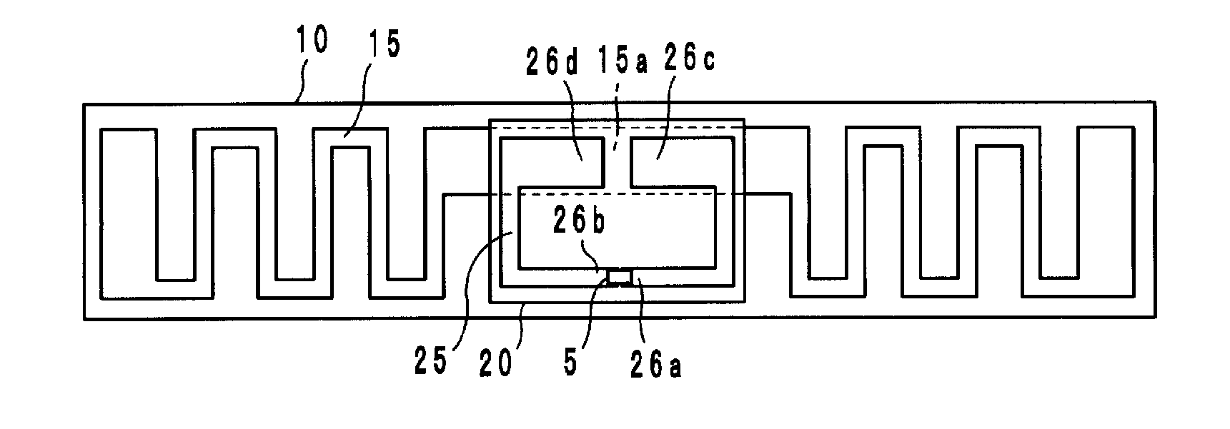
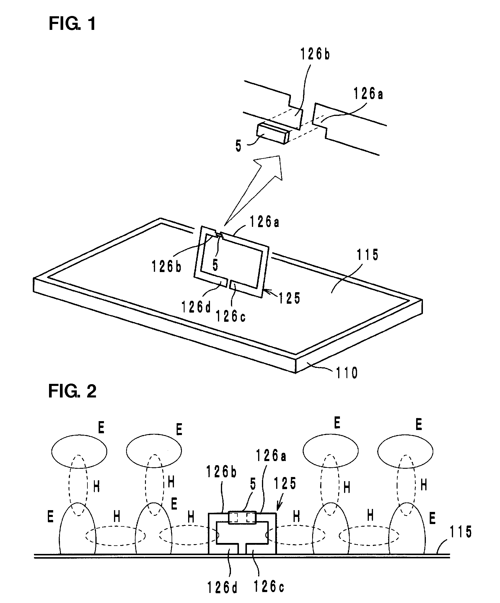
[0039]A wireless IC device according to a first preferred embodiment of the present invention preferably includes a wireless IC chip 5 arranged to process transmission and reception signals having certain frequencies, a radiation plate 115 provided on a base 110, such as a polyethylene terephthalate (PET) film, for example, and a coupling electrode 125 provided on a base (not shown), such as a PET film, for example, as shown in FIG. 1.

[0040]The coupling electrode 125 preferably includes a pair of coupling portions 126a and 126b to be coupled to the wireless IC chip 5 and a pair of opposing ends 126c and 126d defined by a cutout of the coupling electrode 125. The wireless IC chip 5 preferably includes, for example, a clock circuit, a logic circuit, and a memory circuit. Necessary information is stored in the wireless IC chip 5. A pair of input-output terminal electrodes (not shown) is provided on the rear surface of the wireless IC chip 5. The pair of input-output terminal electrodes...

second preferred embodiment

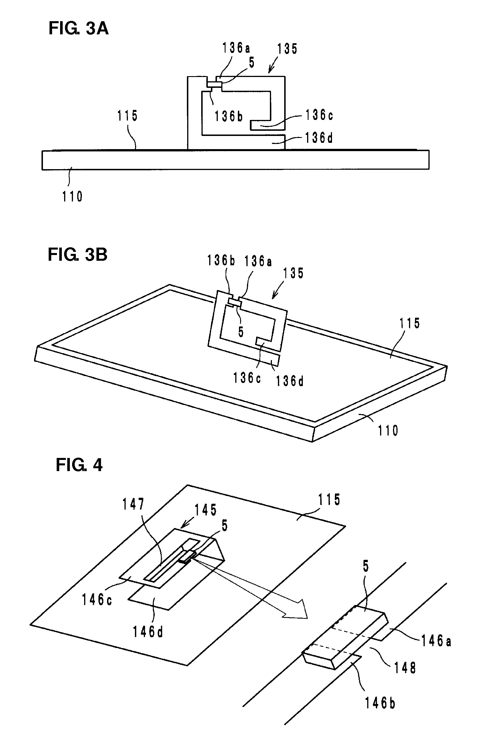
[0052]A wireless IC device component according to a second preferred embodiment of the present invention preferably includes a coupling electrode 135, as shown in FIGS. 3A and 3B. The coupling electrode 135 preferably includes a pair of coupling portions 136a and 136b arranged to be coupled to the wireless IC chip 5 and a pair of opposing ends 136c and 136d. The opposing ends 136c and 136d are capacitively coupled to each other.

[0053]The opposing end 136c is capacitively coupled to the opposing end 136d, so that the coupling electrode 135 electrically forms an annular electrode and functions as a magnetic-field antenna. The wireless IC device component functions as a wireless IC device with the coupling electrode 135 being coupled to the radiation plate 115, similarly to the coupling electrode 125 shown in the first preferred embodiment.

[0054]The coupling electrode 135 has an inductive reactance (XL: jωL) caused by the electrical length and a capacitive reactance (XC: 1 / jωC) caused ...

third preferred embodiment

[0056]A wireless IC device component according to a third preferred embodiment of the present invention preferably includes a coupling electrode 145 having a U-shape in a side view, as shown in FIG. 4. The coupling electrode 145 is preferably provided from the front surface of a base (not shown) made of resin, for example, to the rear surface thereof and includes an opening 147 and a slit 148 extending to the opening 147 on its surface. The opening 147 and the slit 148 define a pair of coupling portions 146a and 146b to be coupled to the wireless IC chip 5. The coupling electrode 145 includes opposing ends 146c and 146d. The opposing ends 146c and 146d are capacitively coupled to each other.

[0057]The opposing end 146c is capacitively coupled to the opposing end 146d, so that the coupling electrode 145 electrically forms an annular electrode, functions as a magnetic-field antenna, and is coupled to the radiation plate 115. The operational effects of the third preferred embodiment are...


PUM


Abstract

A wireless IC device includes a wireless IC chip, a coupling electrode, and a radiation plate. The coupling electrode includes coupling portions arranged to be coupled to the wireless IC chip and a pair of opposing ends. The pair of opposing ends are capacitively coupled to each other and oppose the radiation plate to be coupled to the radiation plate. The wireless IC chip uses the radiation plate as an antenna to transmit and receive signals having certain frequencies to and from an RFID system.

Description

BACKGROUND OF THE INVENTION[0001]1. Field of the Invention[0002]The present invention relates to wireless integrated circuit (IC) device components and wireless IC devices. More particularly, the present invention relates to a wireless IC device component and a wireless IC device preferably for use in a Radio Frequency Identification (RFID) system.[0003]2. Description of the Related Art[0004]Hitherto, RFID systems have been developed as article management systems. In such an RFID system, a reader-writer producing an induction electromagnetic-field communicates with an IC chip (also referred to as an IC tag or a wireless IC chip) in a non-contact manner. The IC chip is attached to, for example, an article or a container and stores certain information to be transmitted. The IC chip is coupled to an antenna, that is, a radiation plate to enable communication with the reader-writer.[0005]Japanese Registered Utility Model No. 3148168 discloses a wireless IC device which includes a wirele...

Claims


Application Information

Patent Timeline
Patent Type & Authority Patents(United States)
IPC IPC(8): G06K19/06
CPCG06K19/07749G06K19/07756H01Q1/2225G06K19/07754H01Q9/26H01Q9/285H01Q7/00H01L2224/16225
Inventor KATO, NOBORUDOKAI, YUYA
Owner MURATA MFG CO LTD
Why Eureka
Try Eureka