Simplified silicon drift detector and wraparound neutron detector

a technology of drift detector and silicon solid state detector, which is applied in the field of radiation detection, can solve the problems of large area sdds (i.e., >100 mmsup>2/sup>), other significant limitations, and pronounced spread between drifting electrons, so as to reduce ballistic deficit and shorten drift distance

Active Publication Date: 2013-04-16
CANBERRA IND INC
View PDF10 Cites 4 Cited by
  • Summary
  • Abstract
  • Description
  • Claims
  • Application Information

AI Technical Summary

Benefits of technology

[0011]The present invention includes various embodiments of large area SDD detectors. In one embodiment, the detector features linear anodes and oblong-shaped steering electrodes surrounding the linear anodes. This embodiment is useful for applications requiring direct detection of ionizing radiations such as alphas, betas, and X-rays. The dimensions of these linear anode devices possess aspect ratio of L / W dimensions higher then 2, provides shorter drift distances then with circular devices having the same active area and therefore reduces ballistic deficit.
[0012]Another embodiment includes a central anode SDD drift detector (such as oblong, circular, hexagonal or rectangular drift detectors shapes) utilizing a biasing configuration wherein the irradiation and anode stop rings (edge electrodes) are set at the same reverse bias. This embodiment comprises an additional ring between p+ electrode and the irradiation side stop ring and / or an additional ring between the HV steering electrode and the anode side stop ring, in order to prevent injection current from the edge to the active area.
[0013]The embodiment may also comprise a continuous P+ junction on the irradiation side. The bias of this continuous junction in such a configuration is the same as the bias of anode side stop ring. The continuous junction and anode side stop ring can be linked together in order to reduce the resistance between them.
[0014]In another embodiment the SDD linear anode drift detector comprises a periodic array of rectangular anodes (which can be monolithic or separate devices). This configuration is useful for applications where the detectors are coupled to scintillators. The scintillators can then either convert gammas to visual photons (e.g., CsI, LaBr, and NaI) or neutrons to visual photons (LiF). The advantage of this approach is that for a given area, if the L / W ratio is large enough, the drift length of electrons will be smaller than for a circular drift detector, enabling the use if lower shaping times.
[0017]The present invention also includes a low capacitance detector for neutron detection wherein the p+ electrode surrounding the anode is implemented in a wrap around geometry. The advantage of such a wrap around geometry is that the electron drift time is smaller than for a simple planar interdigitated simplified SDD detector. An additional advantage is that they are compatible with texturing.

Problems solved by technology

However, very large area SDDs (i.e., >100 mm2) face other significant limitations.
One such limitation is the ballistic deficit.
This repulsion results in a pronounced spread between the drifting electrons.
This spread does not allow all electrons to reach the anode at the same time.
Consequently, larger shaping times must be utilized by the detection circuitry which further limits the practical size of the SDDs.
A larger shaping time also reduces count rate performance due to the influence of leakage current.

Method used


Image

  • Simplified silicon drift detector and wraparound neutron detector
  • Simplified silicon drift detector and wraparound neutron detector
  • Simplified silicon drift detector and wraparound neutron detector

Examples


Embodiment Construction

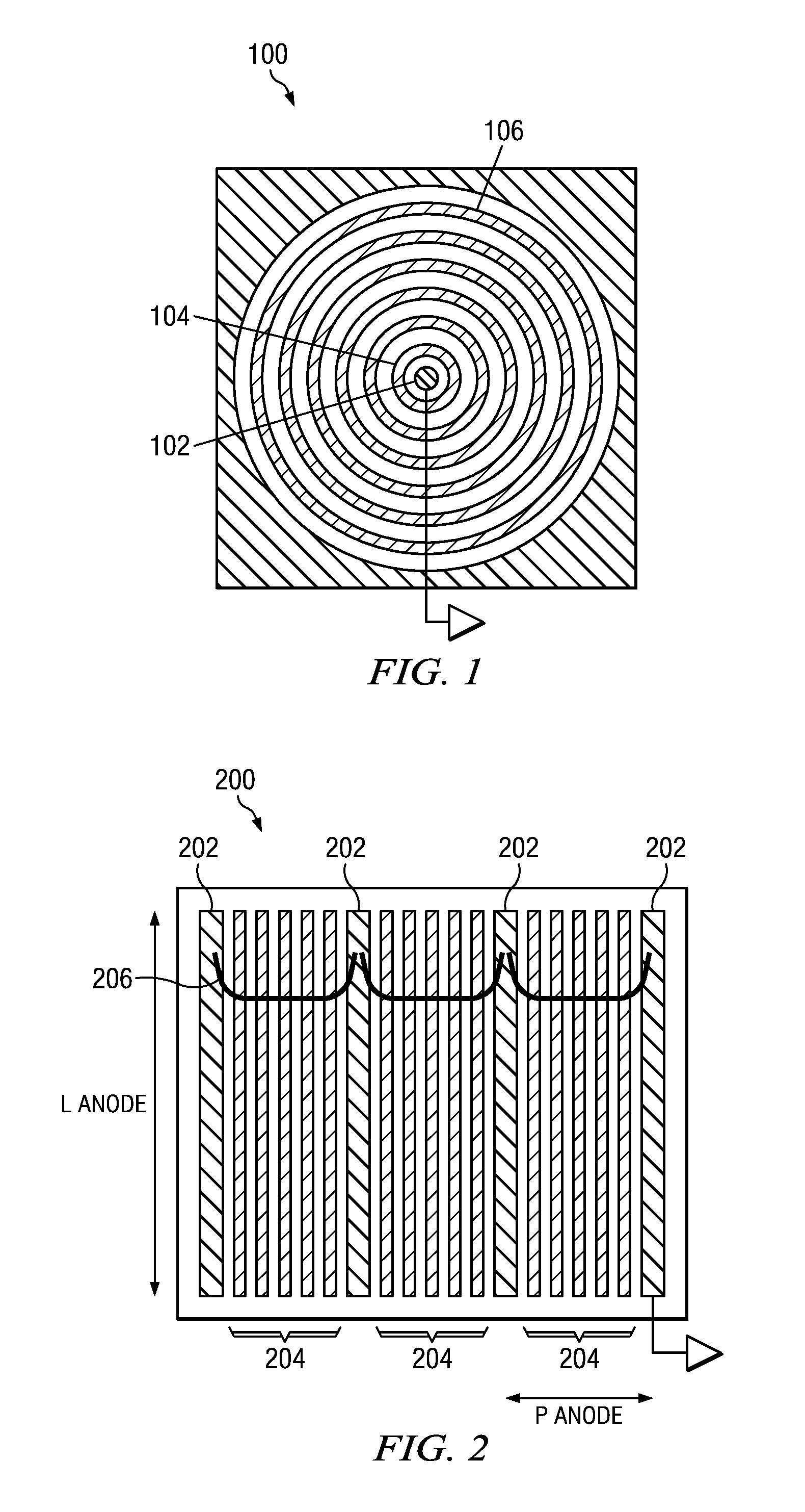
[0062]FIG. 1 depicts a traditional SDD (100) having a small circular anode (102) at its center. By keeping the center anode (102) smaller relative to the overall area of the detector, capacitance of the detector can be minimized. This minimization reduces the series-noise component and thus reduces (i.e., improves) the overall inherent electronic noise of the device. This central anode (102) is then linked to the radiation detection circuitry. A low voltage bias is applied to the inner drift rings (104) with the highest reverse bias is applied to the outer rings (106).

Linear Drift Detector with Linear Anodes

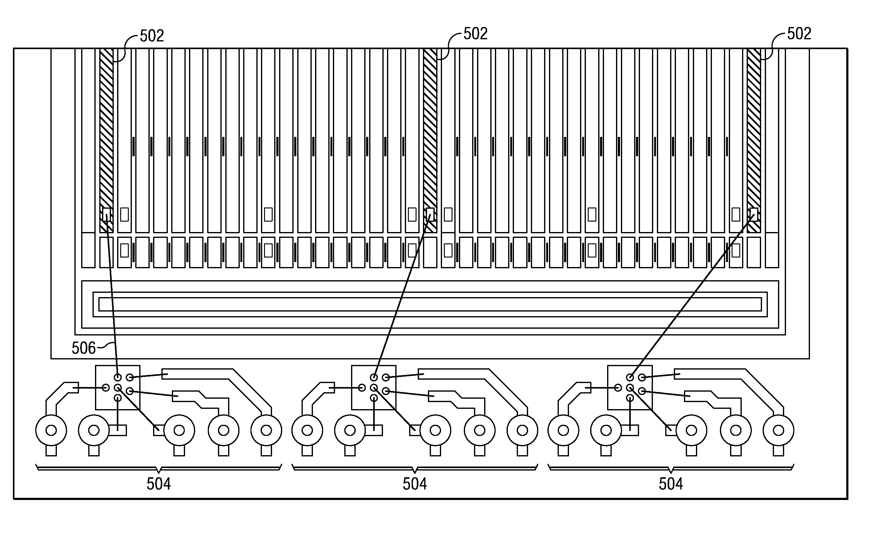
[0063]Another way to reduce the capacitance of SDD detectors is to make drift detector with thin rectangular anodes where the drift structures are linear. Although the capacitance of such detectors tends to be larger than that of a circular SDD, this new anode geometry provides other advantages that more than offset the increased noise. Such a detector is depicted in FIG. 2.

[0064...


PUM


Abstract

A large area SDD detector having linear anodes surrounded by steering electrodes and having an oblong, circular, hexagonal, or rectangular shape. The detectors feature stop rings having a junction on the irradiation side and an ohmic contact on the anode side and / or irradiation side. The irradiation and anode stop ring biasing configuration influences the leakage current flowing to the anode and, hence, the overall efficiency of the active area of the detector. A gettering process is also described for creation of the disclosed SDD detectors. The SDD detector may utilize a segmented configuration having multiple anode segments and kick electrodes for reduction of the detector's surface electric field. In another embodiment, a number of strip-like anodes are linked together to form an interdigitated SDD detector for use with neutron detection. Further described is a wraparound structure for use with Ge detectors to minimize capacitance.

Description

CROSS-REFERENCE TO RELATED APPLICATIONS[0001]This application claims the benefit of provisional Application No. 61 / 226,185, filed Jul. 16, 2009.STATEMENT REGARDING FEDERALLY SPONSORED RESEARCH OR DEVELOPMENT[0002]Not ApplicableTHE NAMES OF THE PARTIES TO A JOINT RESEARCH AGREEMENT[0003]Not ApplicableINCORPORATION-BY-REFERENCE OF MATERIAL SUBMITTED ON A COMPACT DISC[0004]Not ApplicableBACKGROUND OF THE INVENTION[0005]1. Field of the Invention[0006]The present invention relates to radiation detection, and, more specifically, to the detection of ionizing radiation using large area silicon solid state detectors.[0007]2. Description of Related Art including information disclosed under 37 CFR 1.97 and 1.98[0008]Silicon Drift Detectors (SDD) having concentric drift electrodes around an anode on the counter irradiation side and a continuous p+ junction on the irradiation side are known in the art. FIG. 1 depicts such a traditional SDD having such circular anode. The benefit of a small anode...

Claims


Application Information

Patent Timeline
Patent Type & Authority Patents(United States)
IPC IPC(8): H01L21/00
CPCG01T1/2928
Inventor MORICHI, MASSIMOEVRARD, OLIVIERKETERS, MARIJKEBRONSON, FRAZIERMORELLE, MATHIEUBURGER, PAUL
Owner CANBERRA IND INC
Why Eureka
Try Eureka