Hall sensor

a sensor and hall technology, applied in the field of semiconductor hall elements, can solve the problems of inability to increase the ratio w/l to improve the potential distribution of the element's potential generator generates offset voltage, and the inability to eliminate offset voltage using spinning current, etc., to achieve the effect of enhancing the sensitivity of the hall element, eliminating offset voltage, and reducing the potential distribution

Inactive Publication Date: 2013-04-23
ABLIC INC
View PDF7 Cites 5 Cited by
  • Summary
  • Abstract
  • Description
  • Claims
  • Application Information

AI Technical Summary

Benefits of technology

[0022]Further, the Hall sensor according to the present invention is capable of eliminating an offset voltage by spinning current.
[0025]The use of the above-mentioned measures can eliminate the offset voltage by spinning current. Since the control current input terminals and the Hall voltage output terminals are arranged independently to each other, the input terminals can be formed larger while the output terminals can be formed smaller. Further, the distance W between the Hall voltage output terminals can be made larger and the distance L between the control current input terminals can be made smaller. This way, the sensitivity of the Hall element can be enhanced. Besides, the present invention can provide a highly-sensitive Hall sensor capable of eliminating an offset voltage by a single Hall element while having a small chip size.

Problems solved by technology

It is considered that an imbalanced potential distribution inside the element generates the offset voltage due to mechanical stress applied to the element from the outside or due to misalignment occurring in a manufacturing process.
However, in the method of the first one (JP 06-186103 A), unless the currents applied to the Hall sensing portion in two directions or the output Hall voltages therefrom are the same, the offset voltage cannot be eliminated by utilizing spinning current.
Accordingly, there is a problem that the ratio W / L cannot be increased to improve the sensitivity of the Hall element.
However, since a plurality of the Hall elements are used, there is a problem that the chip size increases, leading to an increase in cost.
In addition, the offset voltage elimination by the spinning current is insufficient to eliminate the offset voltage in some cases.

Method used


Image

  • Hall sensor
  • Hall sensor
  • Hall sensor

Examples


Embodiment Construction

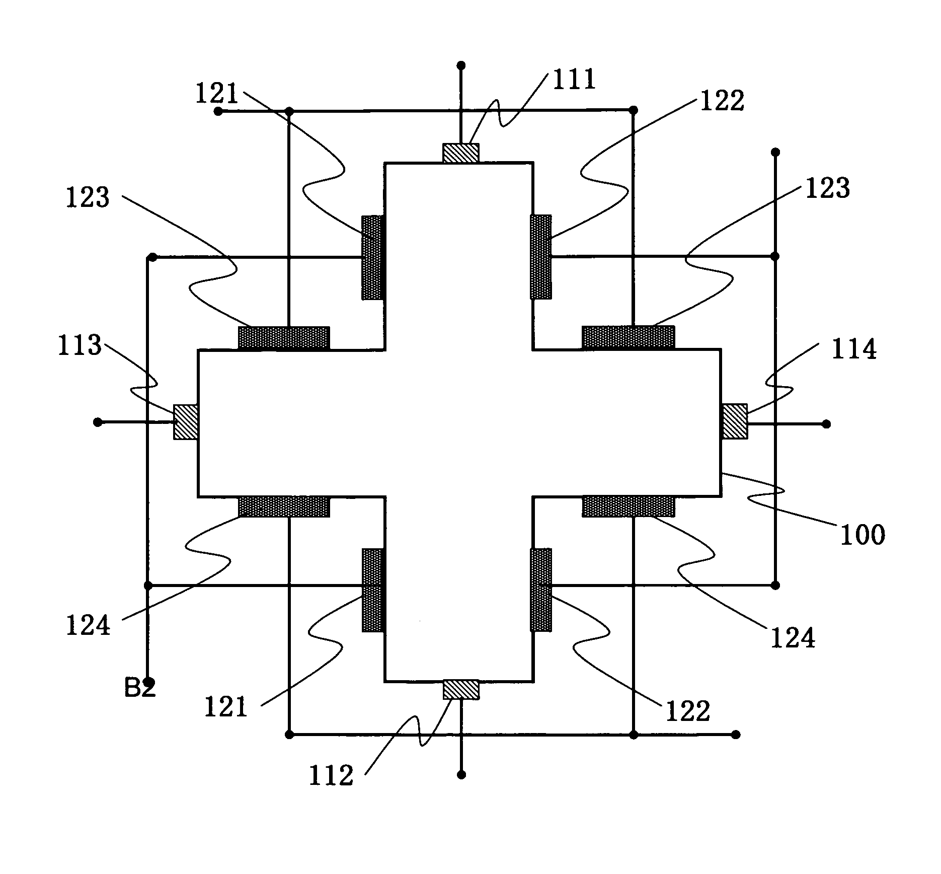
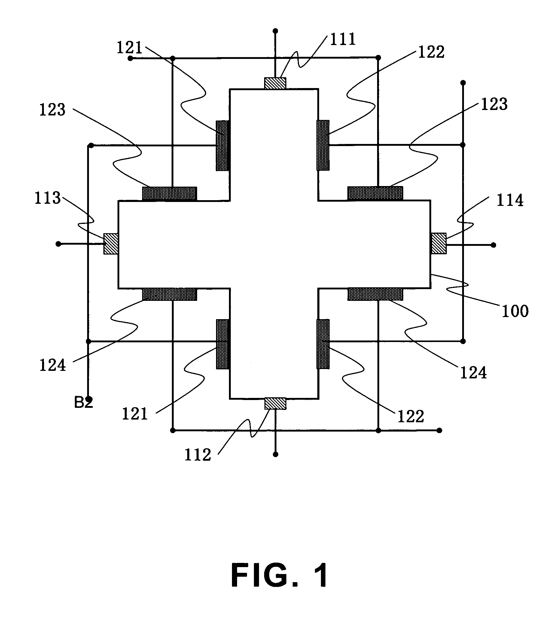
[0033]FIG. 1 is a plan view illustrating a structure of a Hall element according to an embodiment of the present invention. The Hall element of this embodiment includes a Hall sensing portion 100 having shape of a cross and a fourfold axis, rectangular Hall voltage output terminals 111, 112, 113, and 114 at the respective centers of the front edges of four convex portions of the Hall sensing portion 100, and rectangular control current input terminals 121, 122, 123, and 124 in the vicinity of the respective centers of the sides of the convex portions. Of the control current input terminals, control current input terminals arranged in line along the sides of opposed convex portions are connected to each other via metal wiring to have the same potential. Accordingly, two control current input terminals form a pair, and four pairs are provided in total.

[0034]In other words, in this embodiment, as the terminals connected to the Hall element, the Hall voltage output terminals and the con...


PUM


Abstract

Provided is a highly-sensitive Hall element capable of eliminating an offset voltage without increasing the chip size. The Hall element includes: a Hall sensing portion having a shape of a cross and four convex portions; Hall voltage output terminals which are arranged at the centers of the front edges of the four convex portions, respectively; and control current input terminals which are arranged on side surfaces of each of the convex portions independently of the Hall voltage output terminals. In this case, the Hall voltage output terminal has a small width and the control current input terminal has a large width.

Description

BACKGROUND OF THE INVENTION[0001]1. Field of the Invention[0002]The present invention relates to a semiconductor Hall element, and more particularly, to a highly-sensitive Hall sensor capable of eliminating an offset voltage.[0003]2. Description of the Related Art[0004]At first, the principle for detecting magnetism of a Hall element is described. When a magnetic field is applied perpendicularly to a current flowing through a substance, an electric field, which causes a Hall voltage, is generated in a direction perpendicular to both the current and the magnetic field.[0005]Consider a Hall element illustrated in FIG. 2. When the width of a Hall sensing portion 1 which generates the Hall voltage according to the magnetic field is represented by W, the length thereof is represented by L, electron mobility thereof is represented by μ, an applied voltage of a power source 2 for supplying a current is represented by Vdd, and an applied magnetic field is represented by B, the Hall voltage ...

Claims


Application Information

Patent Timeline
Patent Type & Authority Patents(United States)
IPC IPC(8): H01L43/06G01R33/06
CPCH01L43/065G01R33/07H10N52/101G01R15/20
Inventor HIOKA, TAKAAKIOMI, TOSHIHIKO
Owner ABLIC INC
Why Eureka
Try Eureka