Electromagnetic load circuit failure diagnosis device

a technology of electromagnetic load and diagnostic device, which is applied in the direction of electrical control, pulse technique, instruments, etc., can solve the problems of increasing the probability of failure of electromagnetic load circuit including electromagnetic load and driver circuit element, conventionally considered difficult to diagnose, and weak current application, etc., to achieve reliable and accurate detection and improve safety

Active Publication Date: 2013-05-07
HITACHI ASTEMO LTD
View PDF15 Cites 4 Cited by
  • Summary
  • Abstract
  • Description
  • Claims
  • Application Information

AI Technical Summary

Benefits of technology

[0024]The present invention has been made in consideration of the aforementioned problems to be solved, and an object thereof is to provide a failure diagnosis device that detects a layer short-circuit of a switch element such as a FET included in an electromagnetic load circuit and precisely performs a failure diagnosis of the electromagnetic load circuit.

Problems solved by technology

In consideration thereto, there is a recent trend towards an increase in a current applied to an electromagnetic load such as an injector used in an intra-cylinder direct-injection internal-combustion engine, resulting in an increase in the probability of failures in electromagnetic load circuits including an electromagnetic load and a driver circuit element.
However, since a total failure has not yet occurred, a weak current can be applied.
Because a layer short-circuit failure is not a complete breakdown, for example, a current passing through the layer short-circuit failure may be neither excessively large nor excessively small and has conventionally been considered difficult to diagnose.
However, the abnormality detection apparatus performs layer short-circuit detection of an electromagnetic load and is not intended to detect a layer short-circuit of a switch element.
Therefore, the abnormality detection apparatus is incapable of detecting a layer short-circuit of a switch element.
However, this abnormality detection apparatus is similarly not intended to detect an occurrence of a layer short-circuit at a switch element and is incapable of detecting a layer short-circuit of a switch element.
A layer short-circuit of a switch element is not a total failure and is therefore difficult to identify, and as things stand, a failure in an electromagnetic load circuit including a switch element cannot be precisely identified.

Method used


Image

  • Electromagnetic load circuit failure diagnosis device
  • Electromagnetic load circuit failure diagnosis device
  • Electromagnetic load circuit failure diagnosis device

Examples


first embodiment

[0058]A first embodiment of an electromagnetic load circuit failure diagnosis device according to the present invention will now be described with reference to FIGS. 1 and 2.

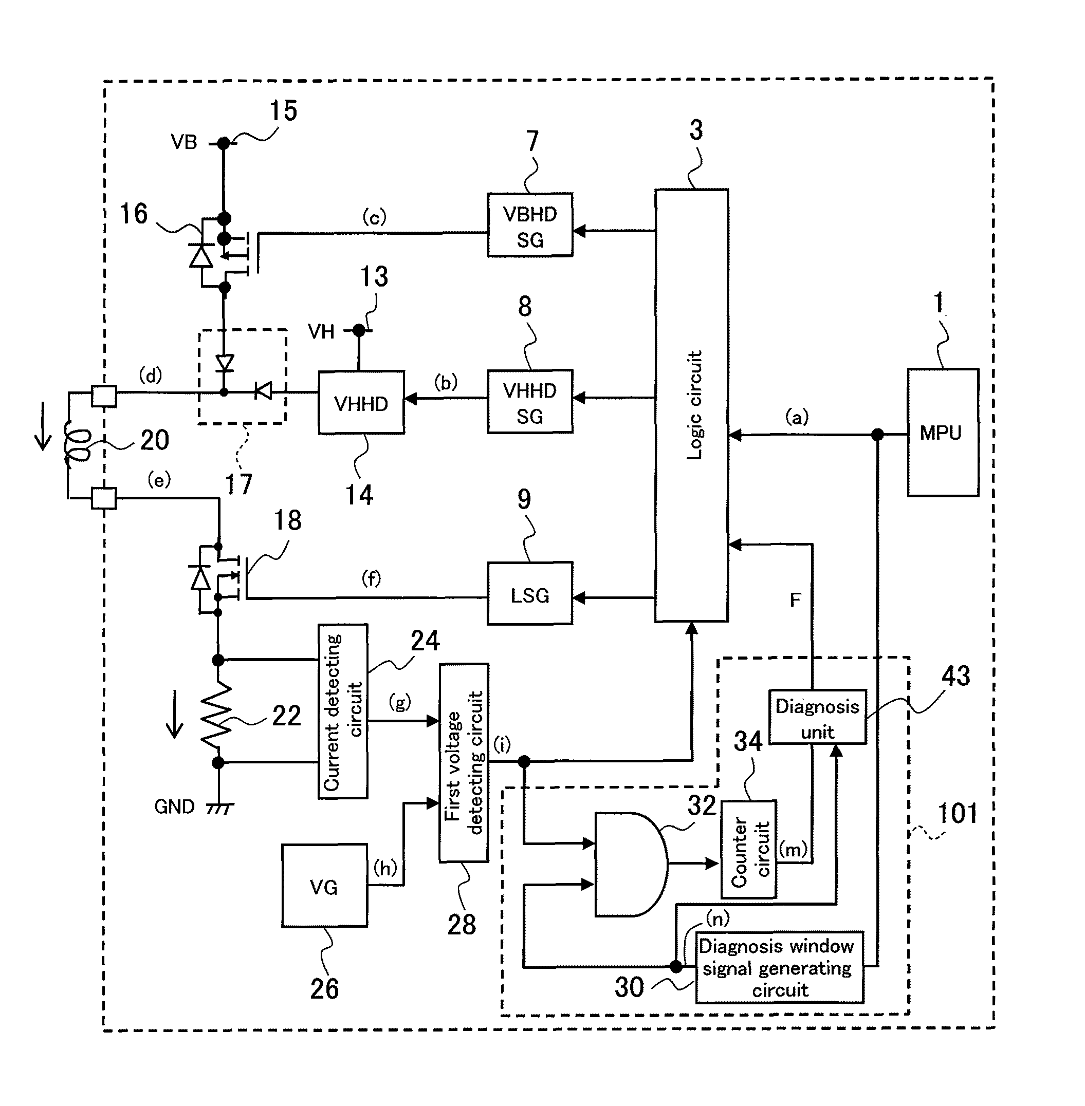
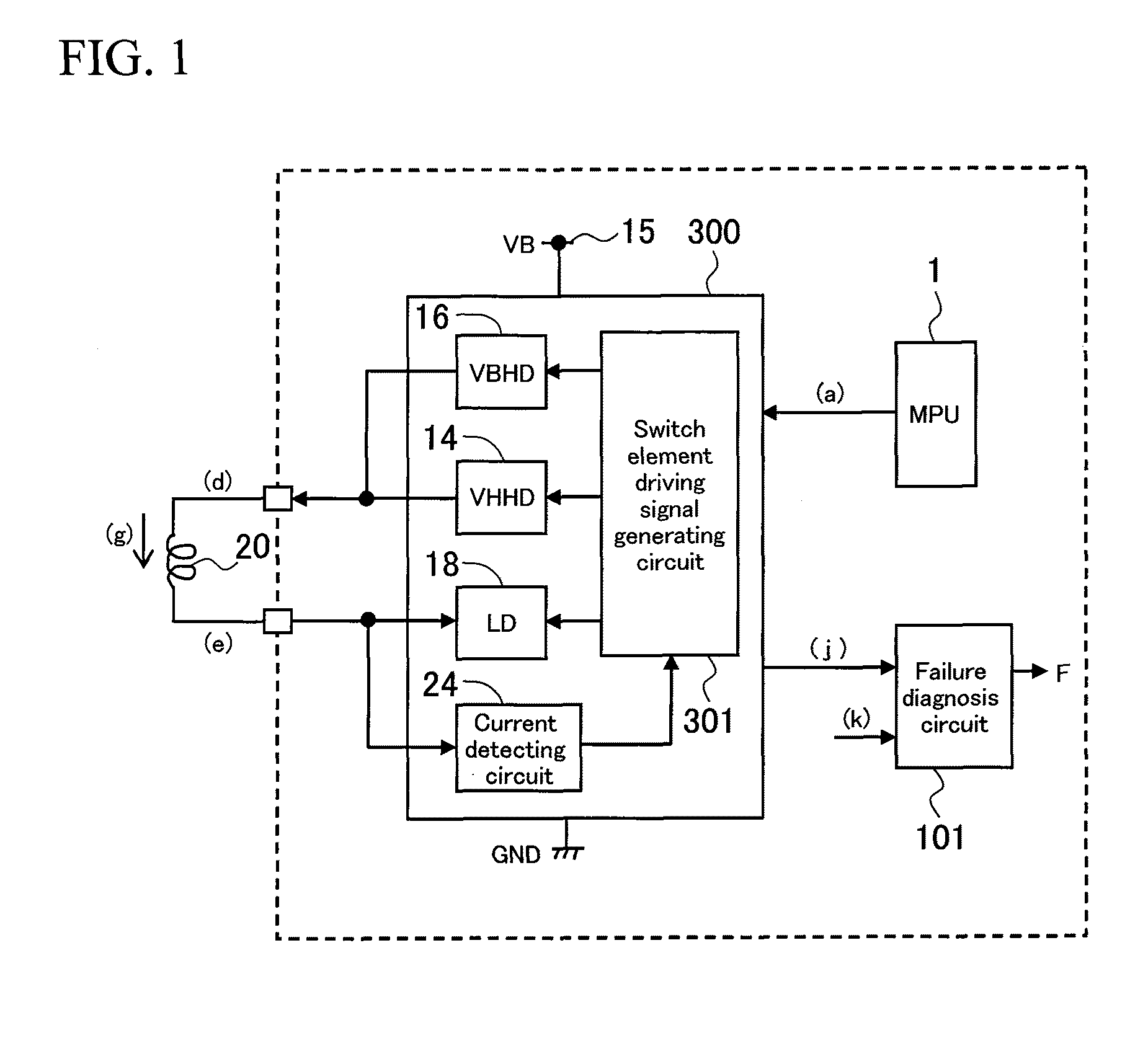
[0059]An electromagnetic load circuit according to the present embodiment includes: an electromagnetic load (injector) 20 installed between a battery voltage terminal 15 and a power supply ground (GND); a microprocessor unit (MPU) 1; an electromagnetic load driving circuit 300; and a failure diagnosis circuit 101.

[0060]A VB high-side driver 16, a VH high-side driver 14, and a low-side driver 18 constituted by switch elements (e.g., FETs) that respectively make up electromagnetic load drivers are installed on the side of the battery voltage terminal 15 and the side of the power supply ground (GND) of the electromagnetic load driving circuit 300 as seen from the electromagnetic load 20.

[0061]In this case, the side of the battery voltage terminal 15 as seen from the electromagnetic load 20 will be referred to as a ...

second embodiment

[0073]A second embodiment (specific example) of an electromagnetic load circuit failure diagnosis device according to the present invention will now be described with reference to FIGS. 3 and 4.

[0074]An electromagnetic load 20 has a positive terminal connected by a VB high-side driver 16 and a VH high-side driver 14, which are switch elements, to any of a power supply terminal 15 with standard voltage (battery voltage, VB) and a high-voltage power supply terminal 13 with a boosting voltage VH and which is boosted to a higher voltage than the battery voltage VB. A diode 17 for backflow prevention is connected between the VB high-side driver 16 and the VH high-side driver 14. A negative terminal of the injector 20 is connected to the ground (GND) via a low-side driver 18 that is a switch element.

[0075]In this case also, the side of a voltage terminal as seen from the electromagnetic load 20 will be referred to as a high side (upstream) and the side of the power supply ground (GND) as ...

third embodiment

[0092]A third embodiment (specific example) of an electromagnetic load circuit failure diagnosis device according to the present invention will now be described with reference to FIGS. 5 and 6.

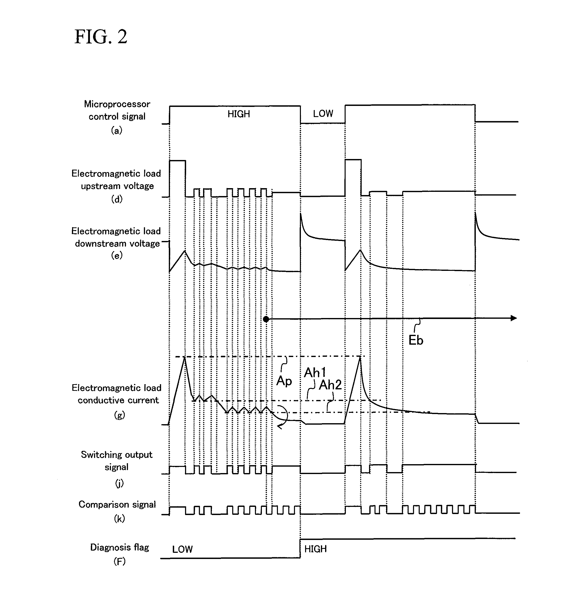
[0093]In the present embodiment, a chopping time processing circuit 42 is provided in place of the counter circuit 34 in the failure diagnosis circuit 101 according to the second embodiment, and a clock signal generating circuit 36 is added. After starting driving at a timing of a rise or a fall of a control signal to be inputted to a switch element driving signal generating circuit, a layer short-circuit failure diagnosis is performed by measuring a period of time needed for a current value of an electromagnetic load 20 to exceed a predetermined threshold.

[0094]Hereinafter, details of the third embodiment will be described. When a layer short-circuit failure Eb occurs at a switch element of a VB high-side driver 16, in the same manner as in the second embodiment, a shunt resistance conductive...


PUM


Abstract

A layer short-circuit of a switch element such as a FET included in an electromagnetic load circuit is detected to accurately perform a failure diagnosis of the electromagnetic load circuit. A failure diagnosis circuit 101 is provided which detects a layer short-circuit in which a high-side switch element, a low-side switch element, or an electromagnetic load itself short-circuits with a power supply voltage terminal or a ground in a state of having a predetermined impedance to perform a failure diagnosis.

Description

TECHNICAL FIELD[0001]The present invention relates to an electromagnetic load circuit failure diagnosis device. In particular, the present invention relates to a failure diagnosis device for a circuit including an electromagnetic load (inductance load) of a fuel injection valve of an internal-combustion engine or the like.BACKGROUND ART[0002]Internal-combustion engines fueled by gasoline, light oil, or the like and which are used in automobiles, motorcycles, agricultural machinery, industrial machinery, marine engines, and the like include those designed to improve fuel efficiency and output by directly injecting fuel into a cylinder using an injector (fuel injection valve).[0003]Since such intra-cylinder direct-injection internal-combustion engines supply an injector with fuel pressurized to a higher pressure than in conventional systems and inject high-pressure fuel into a cylinder from the injector, a significant amount of energy (valve-opening electromagnetic force) is required ...

Claims


Application Information

Patent Timeline
Patent Type & Authority Patents(United States)
IPC IPC(8): G01R31/02
CPCF02D41/20F02D41/22H03K17/0822F02D2041/2058F02D2041/2093Y02T10/40H03K17/18
Inventor OURA, RYOICHIWATANABE, MITSUHIKOMAYUZUMI, TAKUYA
Owner HITACHI ASTEMO LTD
Why Eureka
Try Eureka