Method of constructing inductors and transformers

a transformer and inductor technology, applied in the direction of magnets, inductances, magnetic bodies, etc., can solve the problems of large power converters, unable to meet the needs of high-volume production, and the operation of milling such apertures in pwbs is generally more expensive mechanically

Active Publication Date: 2013-05-21
INFINEON TECH AUSTRIA AG
View PDF24 Cites 16 Cited by
  • Summary
  • Abstract
  • Description
  • Claims
  • Application Information

AI Technical Summary

Problems solved by technology

Milling of such apertures in a PWB is generally a more costly mechanical operation than, for example, drilling of holes.
However, such power converters are generally larger than the needs of the more challenging markets for compact circuit devices, particularly for low power applications, and are produced at costs that do not meet the needs of high-volume production.
However, the overall process is not practical for a high-volume, low-cost production sequence in view of the complexity of the manufacturing steps that are necessary to produce a workable product.

Method used


Image

  • Method of constructing inductors and transformers
  • Method of constructing inductors and transformers
  • Method of constructing inductors and transformers

Examples


Embodiment Construction

[0017]The making and using of the presently preferred embodiments are discussed in detail below. It should be appreciated, however, that the present invention provides many applicable inventive concepts that can be embodied in a wide variety of specific contexts. The specific embodiments discussed are merely illustrative of specific ways to make and use the invention, and do not limit the scope of the invention.

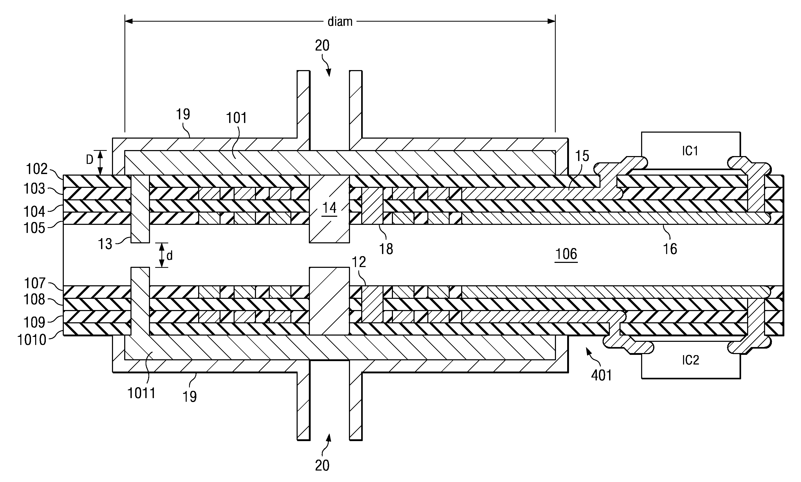
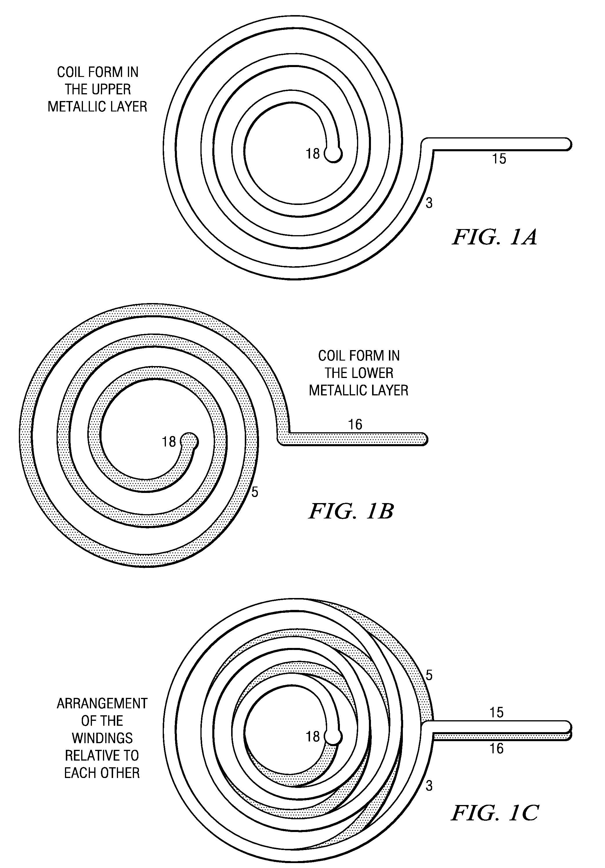
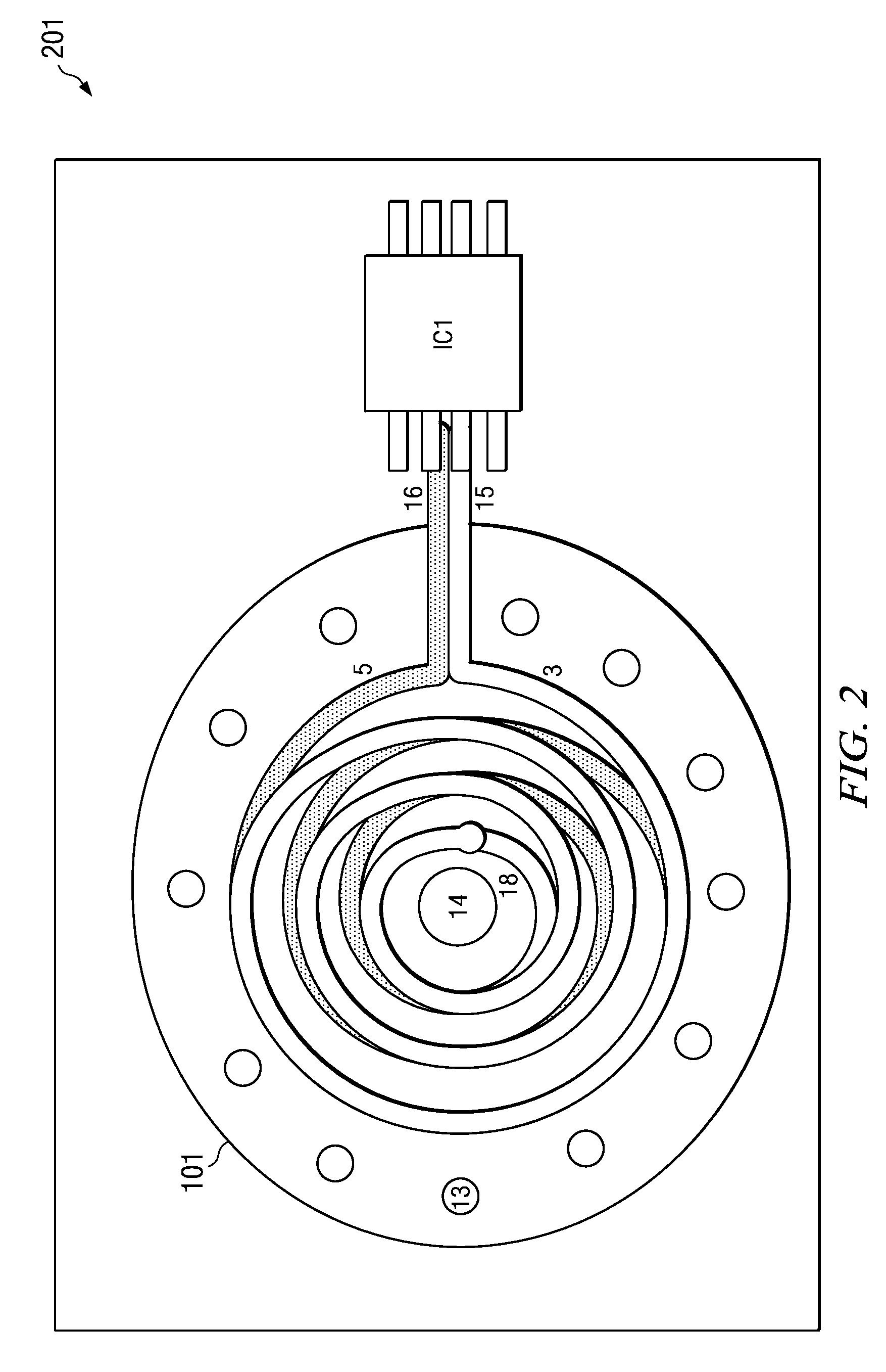
[0018]The present invention will be described with respect to exemplary embodiments in a specific context, namely a magnetic device formed on a substrate with planar windings that produce a magnetic field enhanced by a molded ferromagnetic structure.

[0019]An embodiment of the invention may be applied to various electronic power conversion arrangements, for example, to an integrated isolated or nonisolated power converter configured to power an electronic load. Other devices including a magnetic element can be constructed and applied using processes as introduced herein in dif...


PUM

PropertyMeasurementUnit
metallicaaaaaaaaaa
insulatingaaaaaaaaaa
electrically insulatingaaaaaaaaaa

Abstract

An embodiment of the invention relates to an apparatus including a magnetic device and a related method. A multilayer substrate is constructed with a winding formed in a metallic layer, an electrically insulating layer above the metallic layer, and a via formed in the electrically insulating layer to couple the winding to a circuit element positioned on the multilayer substrate. A depression is formed in the multilayer substrate, and a polymer solution, preferably an epoxy, containing a ferromagnetic component such as nanocrystaline nickel zinc ferrite is deposited within a mold positioned on a surface of the multilayer substrate above the winding and in the depression. An integrated circuit electrically coupled to the winding may be located on the multilayer substrate. The multilayer substrate may be a semiconductor substrate or a printed wiring board, and the circuit element may be an integrated circuit formed on the multilayer substrate.

Description

TECHNICAL FIELD[0001]An embodiment of the invention relates generally to constructing magnetic devices, and in particular, to forming a magnetic device such as an inductor or a transformer on a substrate, such as a printed wiring board or a semiconductor substrate.BACKGROUND[0002]With the increasing complexity and level of integration of electronic products, there is a growing need for distributed and independent power conversion devices, such as point-of-load voltage sources, to provide the well-regulated bias voltages for the highly integrated semiconductor devices that are commonly used. Highly integrated semiconductor devices frequently operate from specialized bias voltages. The power conversion devices must be economical and formed with very small dimensions to meet the size and portability needs of these markets, particularly markets that include portable and compact products such as cellular telephones and personal computers.[0003]A power converter is conventionally formed w...

Claims


Application Information

Patent Timeline
Patent Type & Authority Patents(United States)
IPC IPC(8): H01F5/00H01L21/00H01F17/04
CPCH01F17/0013H01F41/046H01F27/2804H05K1/165H01F2017/002H01F2017/0066H05K1/0298Y10T29/4902H05K2201/0187H05K2201/086H05K2201/09672
Inventor STRZALKOWSKI, BERNHARDSEIBT, MARCOSCHWARZER, ULRICH
Owner INFINEON TECH AUSTRIA AG
Why Eureka
Try Eureka