Semiconductor laser drive device, semiconductor laser drive method, light transmission device, optical wiring module, and electronic device

a laser drive and semiconductor technology, applied in semiconductor lasers, laser details, electrical devices, etc., can solve the problems of difficult power consumption reduction, inability to carry out transmission, and inability to reduce the power consumption of laser drives, so as to improve the transmission performance and light output, the effect of reducing the power consumption of semiconductor lasers

Inactive Publication Date: 2013-06-04
ORMON CORP
View PDF33 Cites 3 Cited by
  • Summary
  • Abstract
  • Description
  • Claims
  • Application Information

AI Technical Summary

Benefits of technology

[0034]One or more embodiments of the present invention provide a semiconductor laser drive device enabling lower cost, space saving, and lower power of the semiconductor laser, and obtaining satisfactory transmission characteristics and light output on the reception side over the entire drive temperature range in the drive of the semiconductor laser.
[0091]Therefore, lower cost, space saving, and lower power of the semiconductor laser are realized, and satisfactory transmission characteristics and light output are obtained on the reception side over the entire drive temperature range in the drive of the semiconductor laser.

Problems solved by technology

However, the technique disclosed in Patent Document 3 has a problem in that reducing the power consumption is difficult.
If the bias current is lower than the threshold current, oscillation delay occurs when performing a high speed transmission of 1 Gbps order, the laser drive itself becomes impossible, and transmission may not be carried out.
Thus, the minimum required drive current becomes extremely large to ensure the extinction ratio when the drive temperature is low temperature, resulting in a problem that the power consumption greatly increases.

Method used


Image

  • Semiconductor laser drive device, semiconductor laser drive method, light transmission device, optical wiring module, and electronic device
  • Semiconductor laser drive device, semiconductor laser drive method, light transmission device, optical wiring module, and electronic device
  • Semiconductor laser drive device, semiconductor laser drive method, light transmission device, optical wiring module, and electronic device

Examples


first embodiment

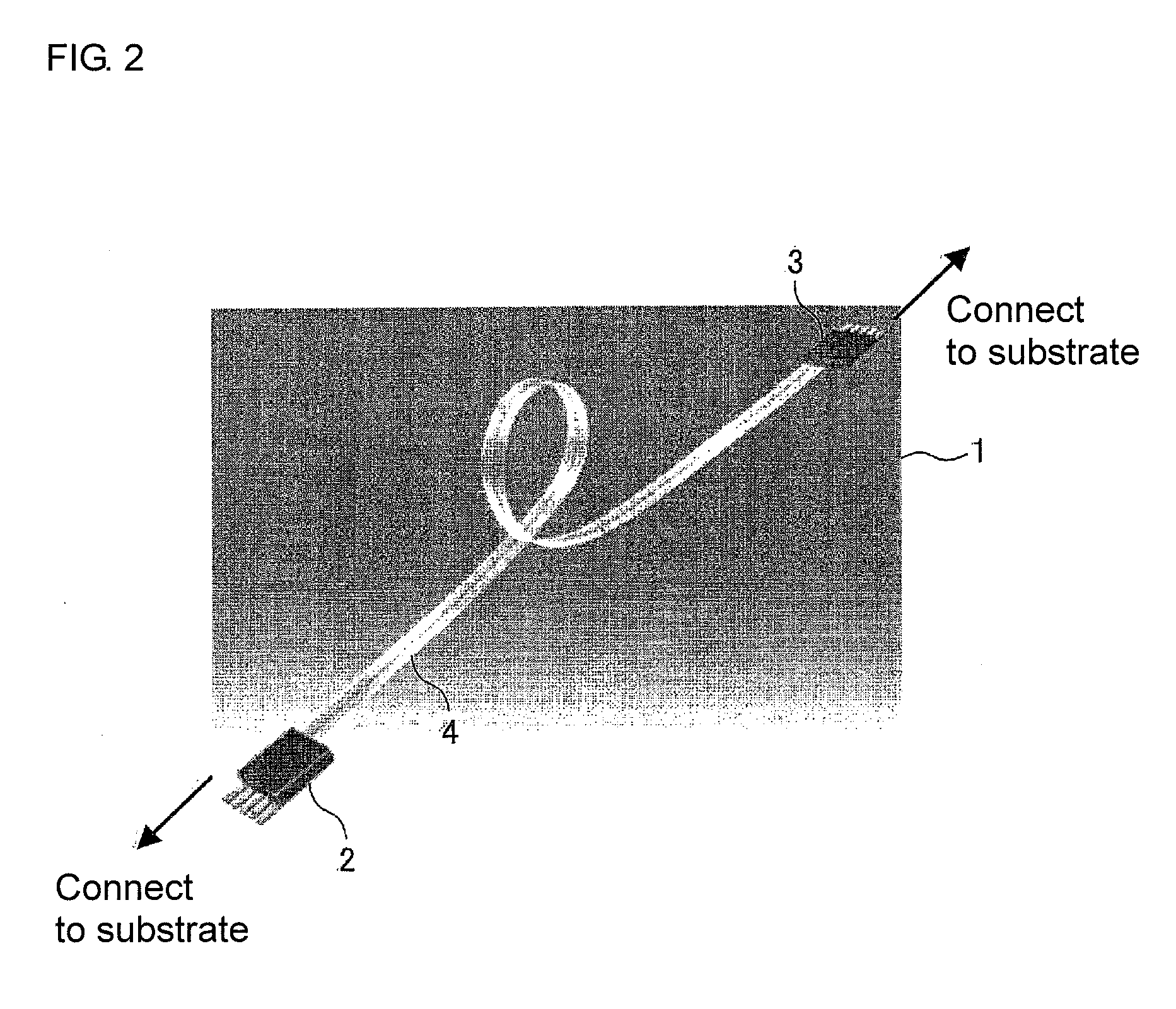
[0115]FIG. 2 shows a schematic view of an optical wiring module.

[0116]The optical wiring module 1 shown in FIG. 2 includes a light transmission device 2, a light reception device 3, and a light guide (transmission medium) 4 having high bendability, and connects a liquid crystal drive circuit substrate and a signal processing circuit substrate in a portable telephone, and the like.

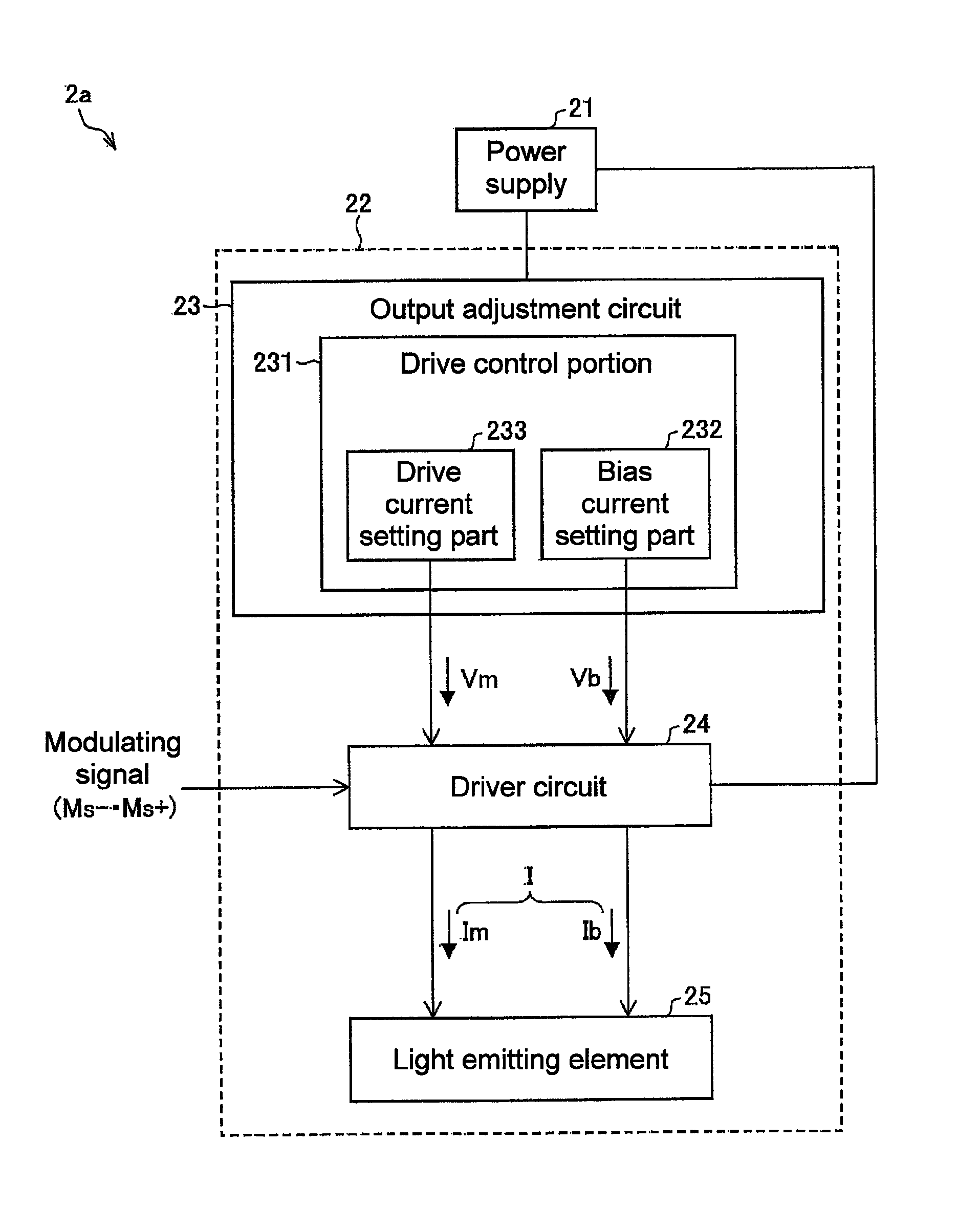
[0117]The light transmission device 2 includes a surface emitting semiconductor laser drive circuit (integrated circuit, drive means) and a surface emitting semiconductor laser (semiconductor laser). In the present embodiment and embodiments to be described later, the light transmission device 2 is assumed to include the surface emitting semiconductor laser for the semiconductor laser. The semiconductor laser of the light transmission device 2 is not limited to the surface emitting semiconductor laser. In other words, the semiconductor laser of the light transmission device 2 may be a semiconductor laser of...

second embodiment

[0189]FIG. 6 is a view showing a semiconductor laser drive method according to another embodiment of the present invention. The embodiment shown in FIG. 6 satisfies conditions [1] to [5], similar to the semiconductor laser drive method shown in FIG. 1.

[0190]In the semiconductor laser drive method shown in FIG. 1, the extreme value of the temperature characteristics of the threshold current defined in condition [1] are set in the vicinity of the normal temperature. The temperature characteristics of the threshold current are a curve projecting downward with the vicinity of the normal temperature as the minimum value, as shown in FIG. 4, and the current value of the threshold current is relatively high at both the high temperature side and the low temperature side of the drive temperature range. Thus, it is difficult to sufficiently bring close the curve representing the temperature characteristics of the threshold current and the line representing the temperature characteristics of t...

third embodiment

[0198]A semiconductor laser drive method according to still another embodiment of the present invention will be described with reference to FIGS. 7 and 8.

[0199]In the embodiments described above, the temperature characteristics of the bias current and the drive current are determined focusing mainly on the oscillation delay time when the threshold current has an extreme value. In other words, the power consumption at the time of data communication can be reduced without causing drawbacks in the data communication originating from the oscillation delay by defining conditions [1] to [5] and determining the temperature characteristics of the bias current and the drive current that satisfy all the conditions.

[0200]In the present embodiment, a method of determining the temperature characteristics of the bias current and the drive current focusing mainly on the extinction ratio when the threshold current has an extreme value will be described.

[0201]The circuit configuration of the light t...


PUM


Abstract

A semiconductor laser drive apparatus comprises a bias current setting section (232) which sets a bias current value on the basis of the drive temperature so that the temperature characteristic of the bias current value with respect to the drive temperature may be a linear function having a slope except zero and a drive current setting section (233) for setting the drive current value on the basis of the drive temperature so that the temperature characteristic of the drive current value with respect to the drive temperature may be a function having a slope except zero. The temperature characteristic of the bias current and that of the drive current are functions different from each other. With this, low cost, space-saving, and power-saving of a semiconductor laser are achieved, and a semiconductor laser drive apparatus enabling a good transmission characteristic on the reception side and a high optical output over the whole drive temperature range when driving the semiconductor laser can be provided.

Description

TECHNICAL FIELD[0001]The present invention relates to a semiconductor laser drive device used as a light source when performing data communication by transmission of optical signals between circuit substrates in an information transmission device including a portable telephone.BACKGROUND ART[0002]Currently, an optical communication network enabling large capacity data communication at high speed such as optical communication, optical network, and optical interconnection is expanding. When performing the data communication between substrates in an electronic device with the optical communication network, the communication is performed through the following method.[0003]Specifically, a plurality of substrates in the electronic device is connected by an optical wiring module. The data communication is performed among the substrates by transmitting the optical signal of 1 GHz through the optical wiring module among the plurality of substrates.[0004]In recent years, a method of using a s...

Claims


Application Information

Patent Timeline
Patent Type & Authority Patents(United States)
IPC IPC(8): H01S3/00H01S3/13H01S5/068
CPCH01S5/06804H01S5/183
Inventor HAMANA, KENTAROENAMI, AKIRATERAKAWA, YUKARIUNO, KEISUKEHOSOKAWA, HAYAMI
Owner ORMON CORP
Why Eureka
Try Eureka