Method for processing amorphous carbon film, and semiconductor device manufacturing method using the method

a technology manufacturing method, which is applied in the direction of organic chemistry, coatings, silicon compounds, etc., can solve the problems of high cost of si based low-k film, and deterioration of the film characteristics of amorphous carbon film, etc., to achieve deterioration of adhesion, deterioration of adhesion, and the effect of allowing the amorphous

Inactive Publication Date: 2013-06-11
TOKYO ELECTRON LTD
View PDF27 Cites 2 Cited by
  • Summary
  • Abstract
  • Description
  • Claims
  • Application Information

AI Technical Summary

Benefits of technology

[0017]According to the present invention, a surface modification process is performed with respect to an amorphous carbon film wet-cleaned after being dry-etched, before forming an upper layer of the amorphous carbon film, and thus, the surface of the amorphous carbon film, which has been damaged by the dry-etching and includes a hydroxyl group (an OH group) formed by the wet-cleaning, can be modified, deterioration of adhesion between the amorphous carbon film and a film formed thereon can be prevented, and permittivity of the amorphous carbon film, which is increased due to the OH group, can be recovered. In particular, since a silylation process is performed as the surface modification process so that the hydroxyl group formed on the surface of the amorphous carbon film are replaced with a silyl group, the deterioration of the adhesion with a metal film of the upper layer on the amorphous carbon film or the increase of the permittivity of the amorphous carbon film may be very effectively prevented.

Problems solved by technology

However, since such a Si based low-k film is expensive and has difficulties in performing etching thereon with high selectivity with respect to other films, low-k films which address the above problems are being required.
In addition, due to an oxidation operation by the formed OH group, film characteristics of the amorphous carbon film are deteriorated, e.g., adhesion between the amorphous carbon film and a film formed on the amorphous carbon film may be deteriorated or a permittivity of the amorphous carbon film increases.

Method used


Image

  • Method for processing amorphous carbon film, and semiconductor device manufacturing method using the method
  • Method for processing amorphous carbon film, and semiconductor device manufacturing method using the method
  • Method for processing amorphous carbon film, and semiconductor device manufacturing method using the method

Examples


Embodiment Construction

[0026]Hereinafter, embodiments of the present invention will be described in detail with reference to accompanying drawings.

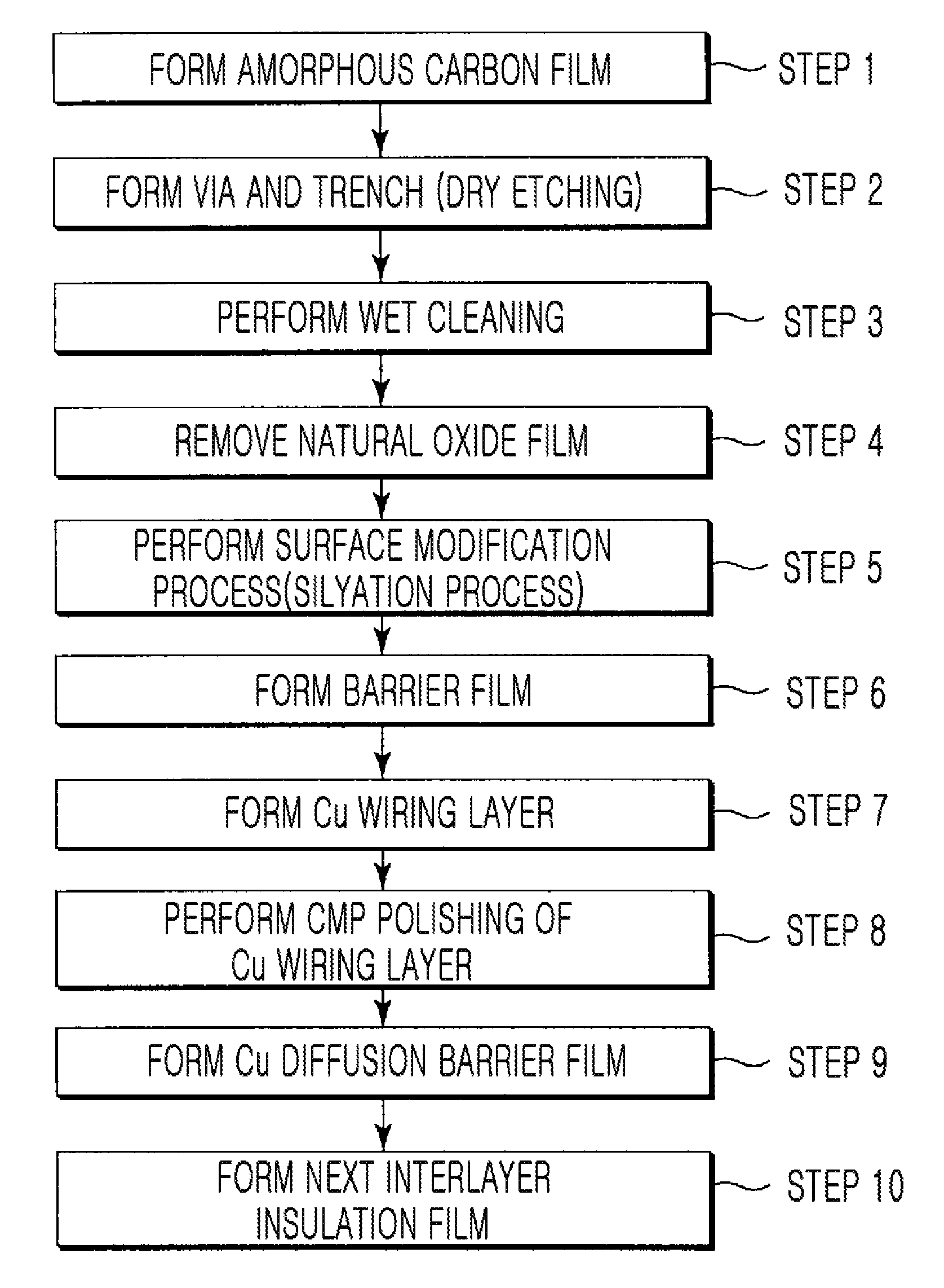
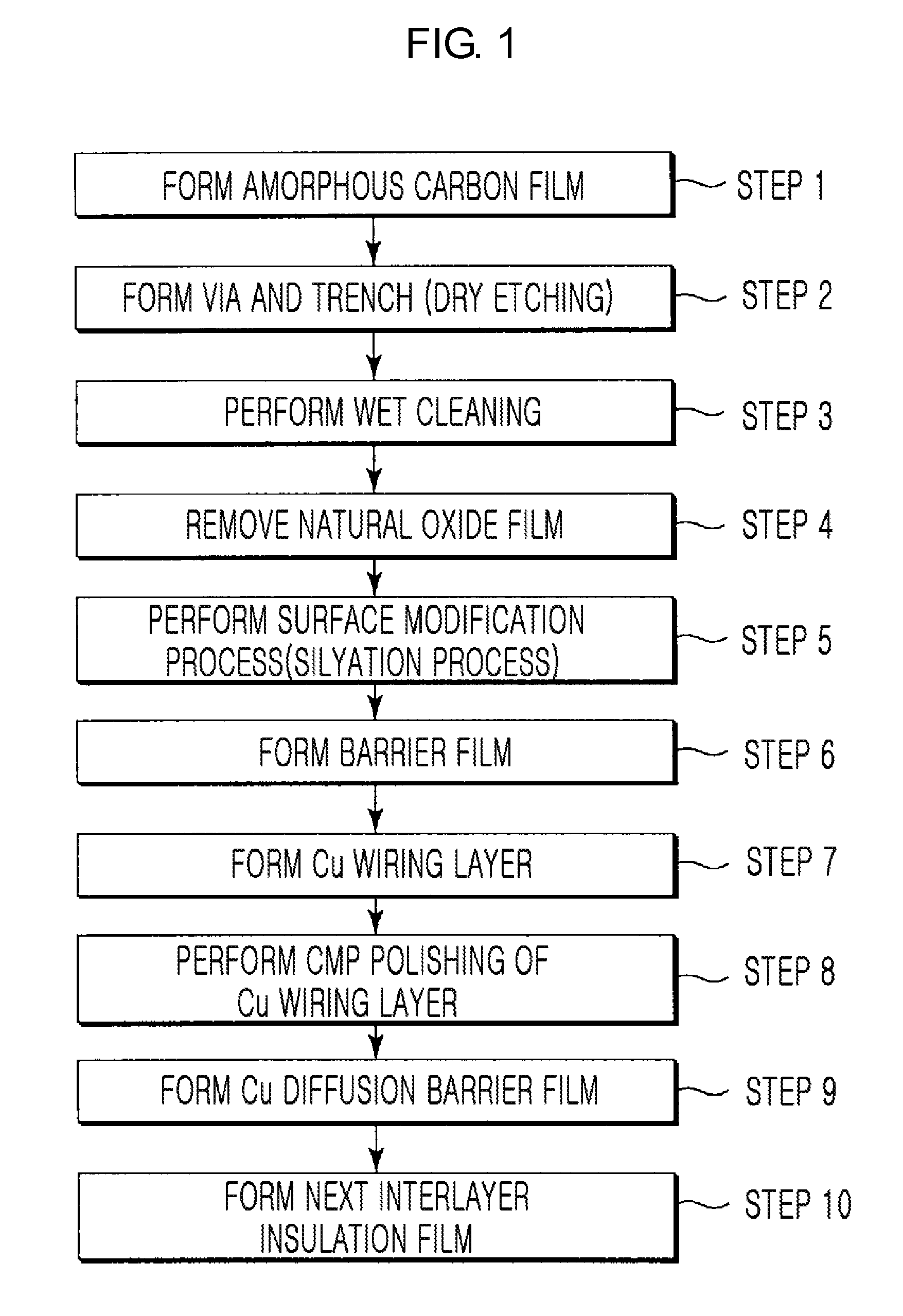
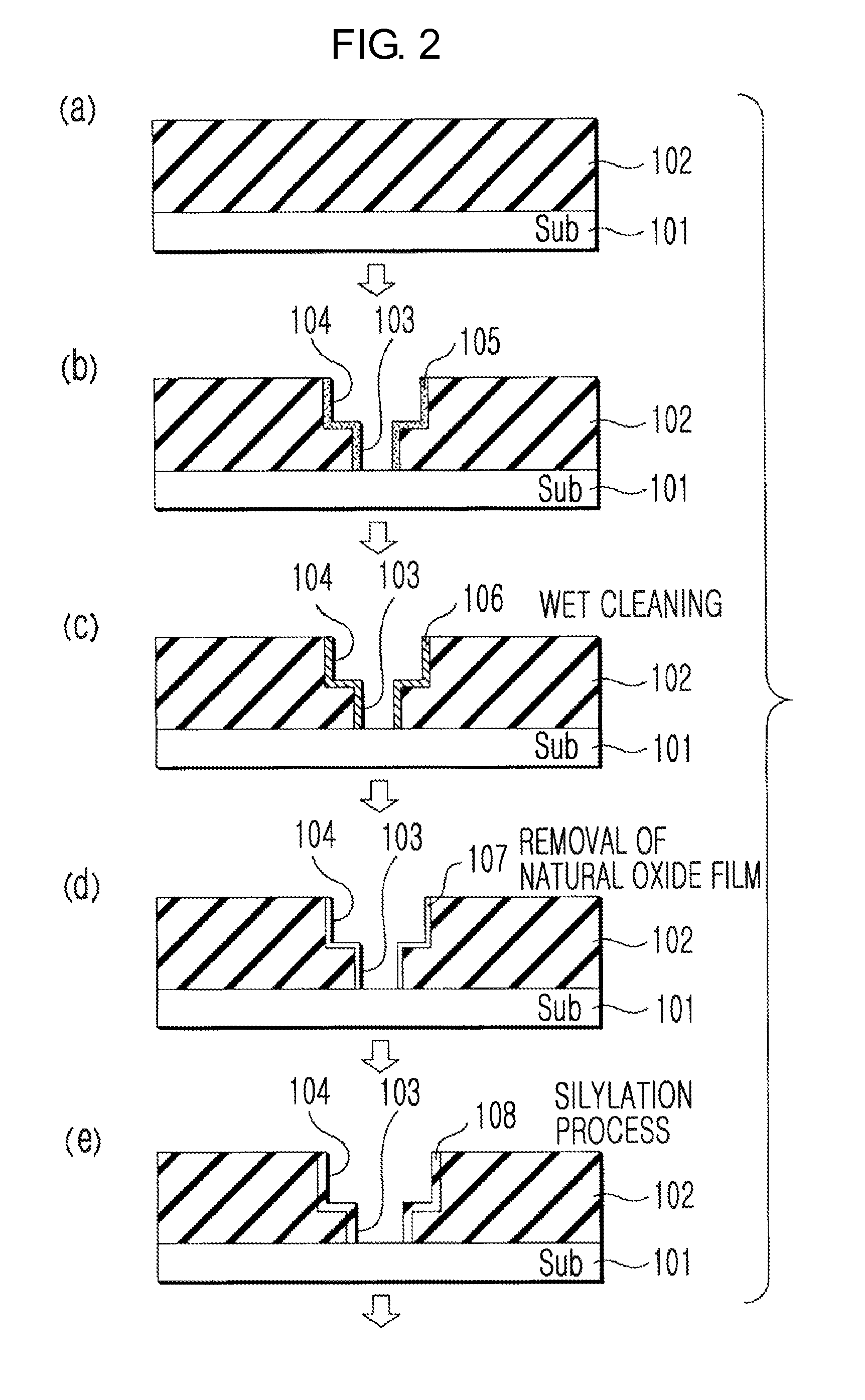
[0027]FIG. 1 is a flowchart showing a series of processes of a semiconductor device manufacturing method including an amorphous carbon film processing method according to an embodiment of the present invention, and FIGS. 2 and 3 are cross-sectional views showing the processes of the semiconductor device manufacturing method.

[0028]According to the present embodiment, first an amorphous carbon film 102 is formed as an interlayer insulation film on a silicon substrate (semiconductor wafer) 101 (step 1, FIG. 2(a)). Although a method of forming the amorphous carbon film 102 is not limited to a certain method, the amorphous carbon film 102 may be preferably formed by CVD, which will be described later. At this time, a hydrocarbon gas, such as propylene (C3H6), propine (C3H4), propane (C3H8), butane (C4H10), butylene (C4H8), butadiene (C4H6), acetylene (C2H2), or the ...


PUM

PropertyMeasurementUnit
temperatureaaaaaaaaaa
pressureaaaaaaaaaa

Abstract

A method for processing an amorphous carbon film which has been formed on a substrate and wet-cleaned after being dry-etched includes preparing the substrate having the wet-cleaned amorphous carbon film and modifying a surface of the amorphous carbon film, before forming an upper layer on the wet-cleaned amorphous carbon film.

Description

TECHNICAL FIELD[0001]The present invention relates to a method for processing an amorphous carbon film which is suitable for a mask or the like when a semiconductor device is manufactured, a semiconductor device manufacturing method using the method.BACKGROUND ART[0002]In a semiconductor device, an interlayer insulation film is formed between wiring layers. In the conventional art, a SiO2 film has been used as such an interlayer insulation film. However, due to recent continuous demands for higher rate of semiconductor devices, a relatively low-permittivity film is demanded. For example, such a low-permittivity interlayer insulation film (low-k film) is formed of a Si based organic material containing Si, O, and C.[0003]However, since such a Si based low-k film is expensive and has difficulties in performing etching thereon with high selectivity with respect to other films, low-k films which address the above problems are being required.[0004]An amorphous carbon film to which hydrog...

Claims


Application Information

Patent Timeline
Patent Type & Authority Patents(United States)
IPC IPC(8): H01L21/00
CPCC23C16/042C23C16/24C23C16/26H01L21/02063H01L21/02115H01L21/02274H01L21/3105H01L21/3146H01L21/76808H01L21/76814H01L21/76831H01L21/76835
Inventor ISHIKAWA, HIRAKUMATSUOKA, TAKAAKI
Owner TOKYO ELECTRON LTD
Why Eureka
Try Eureka