Magneto-resistive effect element having FePt bias magnetic field application layer with Pt seed layer and MgO insulation layer

a magnetic field and magnetic field application layer technology, applied in the field of can solve the problems of /sub>disassembly and modification of the magnetic field application layer, and affecting the effect of magnetic field application

Active Publication Date: 2013-06-11
TDK CORPARATION
View PDF13 Cites 6 Cited by
  • Summary
  • Abstract
  • Description
  • Claims
  • Application Information

AI Technical Summary

Benefits of technology

[0012]By providing the Pt seed layer that is made of an iron-platinum (FePt) alloy on a surface of the Pt seed layer opposite to a surface of the Pt seed layer contacting the hard magnetic layer and in a contact manner with the hard magnetic layer, regularization of the hard magnetic layer can be promoted with a low temperature. Because magnesium (Mg), which configures the MgO insulation film, has higher alloying energy with Pt as compared to Al, Pt is prevented from diffusing into the MgO insulation film. As a result, a decrease in the insulativity of the MgO insulation film is prevented, and a sense current becomes more likely to focus on the MR stack.

Problems solved by technology

However, performing the high temperature annealing causes dispersion of magnetization directions of other ferromagnetic layers, for example, the magnetization pinned layer of the MR stack.
These phenomena interfere with a sense current focusing on the MR stack.
However, Al and Pt are more likely to mix with each other and Pt diffuses into Al2O3, and thereby the insulativity of Al2O3 may decrease or lose.

Method used


Image

  • Magneto-resistive effect element having FePt bias magnetic field application layer with Pt seed layer and MgO insulation layer
  • Magneto-resistive effect element having FePt bias magnetic field application layer with Pt seed layer and MgO insulation layer
  • Magneto-resistive effect element having FePt bias magnetic field application layer with Pt seed layer and MgO insulation layer

Examples


first embodiment

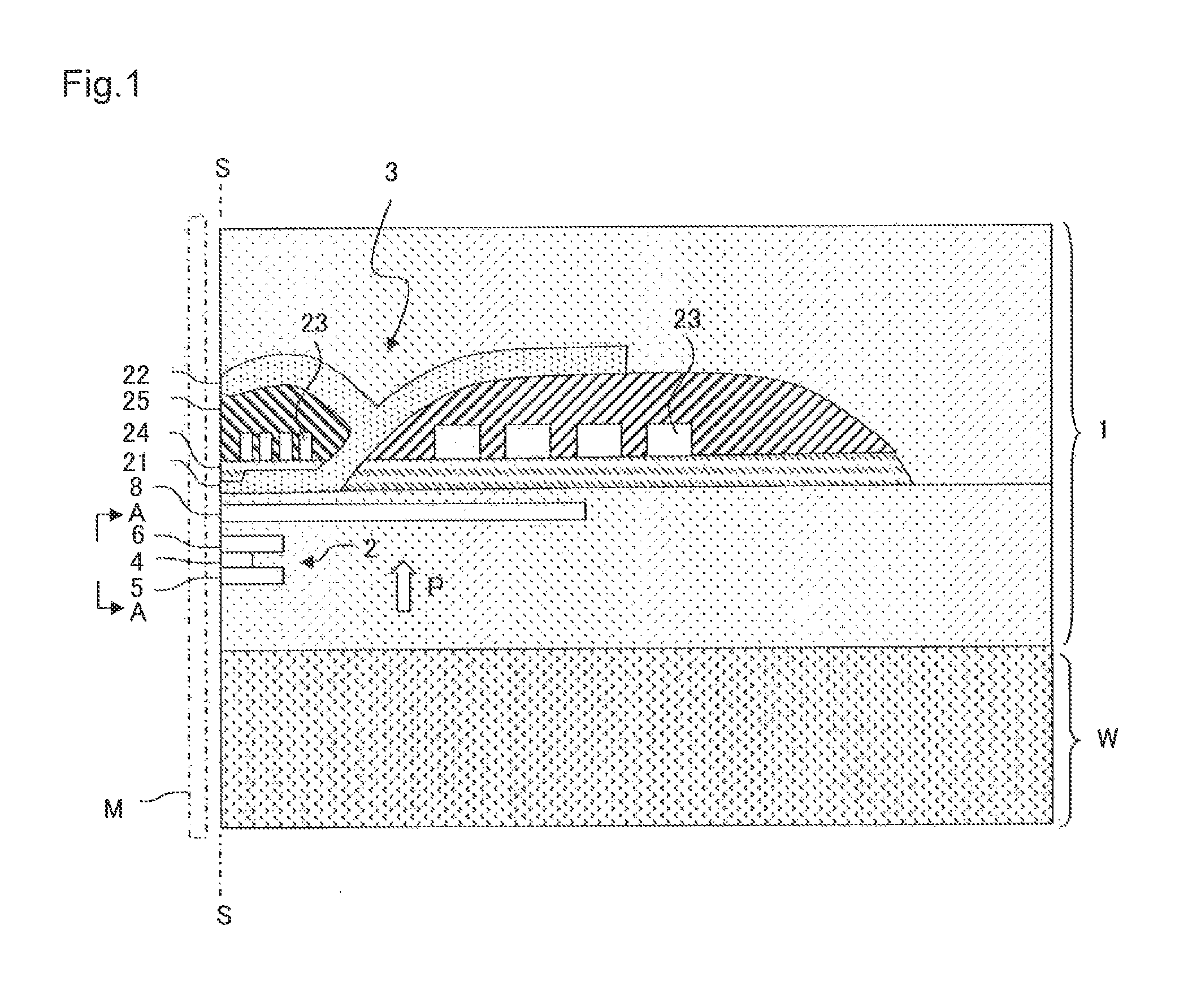
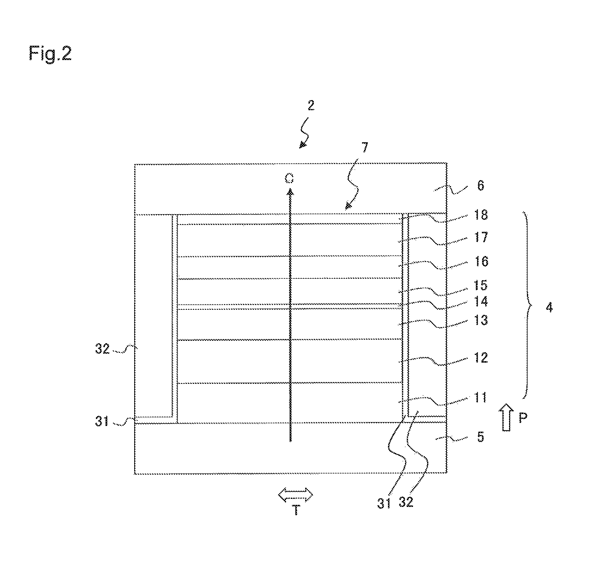
[0028]FIG. 1 illustrates a main part cross-sectional view of a thin film magnetic head 1 according to a first embodiment. The thin film magnetic head 1 is formed on a substrate W and has a reader element 2 and a recording element 3. FIG. 2 is a side view of the reader element 2 from a perspective of an A-A direction of FIG. 1 and illustrates a layer configuration of the reader element 2 on an air bearing surface S. The air bearing surface S is a surface of the thin film magnetic head 1 that faces a recording medium M. First, a description is given of a configuration of the reader element 2 with reference to FIG. 2.

[0029]The reader element 2 has a MR element 4 of a spin valve type, and upper and lower shield layers 6 and 5 that are provided so as to sandwich the MR element 4 in a lamination direction P thereof. The lamination direction P is a direction orthogonal to the MR element 4, specifically film surfaces of a magneto-resistive (MR) stack 7, and orientating from the substrate W ...

second embodiment

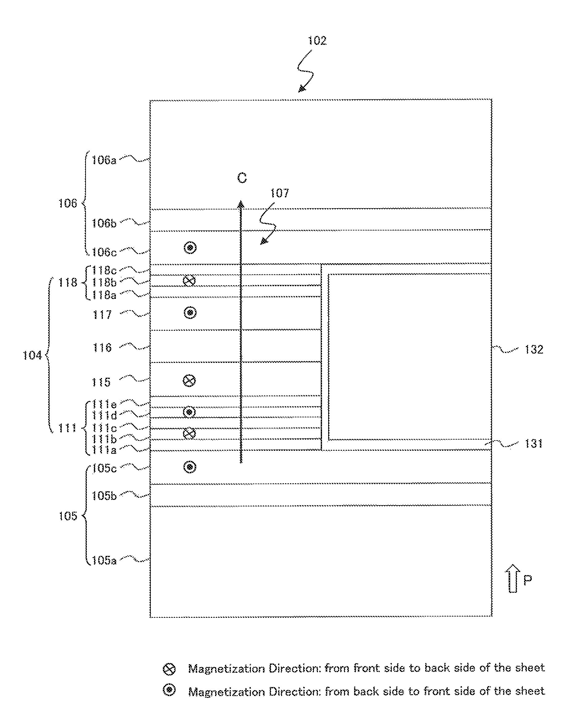
[0051]The thin film magnetic head 1 of the present embodiment is the same as the first embodiment illustrated in FIG. 1 with the exception of a configuration of a reader element 102. FIG. 5 is a side view of the reader element 102 and illustrates a layer configuration of the reader element 102 on the air bearing surface S. Table 2 indicates one example of a layer configuration of a MR stack 107. The reader element 102 has a MR element 104 in which a large number of layers are laminated in the same manner as the first embodiment, and upper and lower shield layers 106 and 105 that are provided so as to sandwich the MR element 104 in the lamination direction P. The MR element 104 has the MR stack 107 through which a sense current C flows, and a bias magnetic field application layer 132 provided on the backside of the MR stack 107 as seen from the air bearing surface S. The upper and lower shield layers 106 and 105 are also used as electrodes for a sense current C so that a sense curren...

example

[0060]Four types of bias magnetic field application layers, each of the types having a different configuration, were arranged on both sides of the MR stacks with respect to the track width direction, and reader elements were configured. An element characteristic and a tolerance with respect to an external magnetic field of the reader elements were evaluated. A process for forming the reader elements used in the present example is indicated in FIGS. 7A-7D. Figures on the right side are plan views, and figures on the left side are cross-sectional views cut along respectively the line A-A through the line D-D illustrated in the plan views.

[0061]Firstly, as illustrated in FIG. 7A, a MR film 207′ is formed on a lower shield layer 205, the MR film 207′ having the same configuration as that of a MR stack 207. Next, as illustrated in FIG. 7B, the MR film 207′ is partially milled, and a track direction width T of the MR stack 207 is formed. At milled portions, which are on the both sides of ...


PUM

PropertyMeasurementUnit
thicknessaaaaaaaaaa
thicknessaaaaaaaaaa
thicknessaaaaaaaaaa

Abstract

A magneto-resistive effect (MR) element includes a magneto-resistive (MR) stack with a magnetization free layer, a bias magnetic field application layer positioned on a side of the MR stack, and an insulation film insulating the bias magnetic field application layer. The bias magnetic field application layer includes hard magnetic layer positioned on the side of the magnetization free layer and formed of iron-platinum (FePt) alloy and Pt seed layer provided between the MR stack and the hard magnetic layer and on a lower surface of the hard magnetic layer in contact manner with the hard magnetic layer and formed of platinum (Pt). The insulation film is a MgO insulation film formed of oxide magnesium (MgO), provided on a surface of the Pt seed layer in contact manner with the Pt seed layer, the surface being opposite to another surface of the Pt seed layer contacting the hard magnetic layer.

Description

BACKGROUND OF THE INVENTION[0001]1. Field of the Invention[0002]The present invention relates to a magneto-resistive effect (MR) element and particularly to a configuration of a bias magnetic field application layer.[0003]2. Description of the Related Art[0004]A MR element used for a hard disk drive (HDD) or the like has a magneto-resistive (MR) stack provided with a magnetization free layer and configured such that a sense current flows therethrough. The magnetization free layer is a magnetic layer of which a magnetization direction changes according to an external magnetic field. The MR stack further has a magnetization pinned layer of which a magnetization direction is pinned, and a spacer layer positioned between the magnetization pinned layer and the magnetization free layer. These three layers change electrical resistance of a sense current based on a MR effect. In another case, the MR stack may have two magnetization free layers and a spacer layer positioned between these mag...

Claims


Application Information

Patent Timeline
Patent Type & Authority Patents(United States)
IPC IPC(8): G11B5/39
CPCG11B5/3932G11B5/398H01L43/08H01L43/12H01F10/123H01F10/30G01R33/093H01F10/3272H01F10/3254H10N50/10H10N50/01
Inventor KANAYA, TAKAYASUSANO, MASASHI
Owner TDK CORPARATION
Why Eureka
Try Eureka