Semiconductor memory device for reducing bit line coupling noise

a memory device and semiconductor technology, applied in the field can solve problems such as interference noise between adjacent bit lines of semiconductor memory devices, and achieve the effect of reducing bit line coupling nois

Active Publication Date: 2013-06-18
SAMSUNG ELECTRONICS CO LTD
View PDF6 Cites 4 Cited by
  • Summary
  • Abstract
  • Description
  • Claims
  • Application Information

AI Technical Summary

Benefits of technology

[0006]An exemplary embodiment of the inventive concept provides a semiconductor memory device for reducing bit line coupling noise.

Problems solved by technology

However, as storage capacity increases, so does interference noise between adjacent bit lines of the semiconductor memory devices.
This noise can impact a voltage margin of a memory cell and a sensing margin of a bit line sense amplifier.

Method used


Image

  • Semiconductor memory device for reducing bit line coupling noise
  • Semiconductor memory device for reducing bit line coupling noise
  • Semiconductor memory device for reducing bit line coupling noise

Examples


Embodiment Construction

[0039]Exemplary embodiments of the inventive concept are described more fully hereinafter with reference to the accompanying drawings. In the drawings, the same reference numerals may denote the same elements.

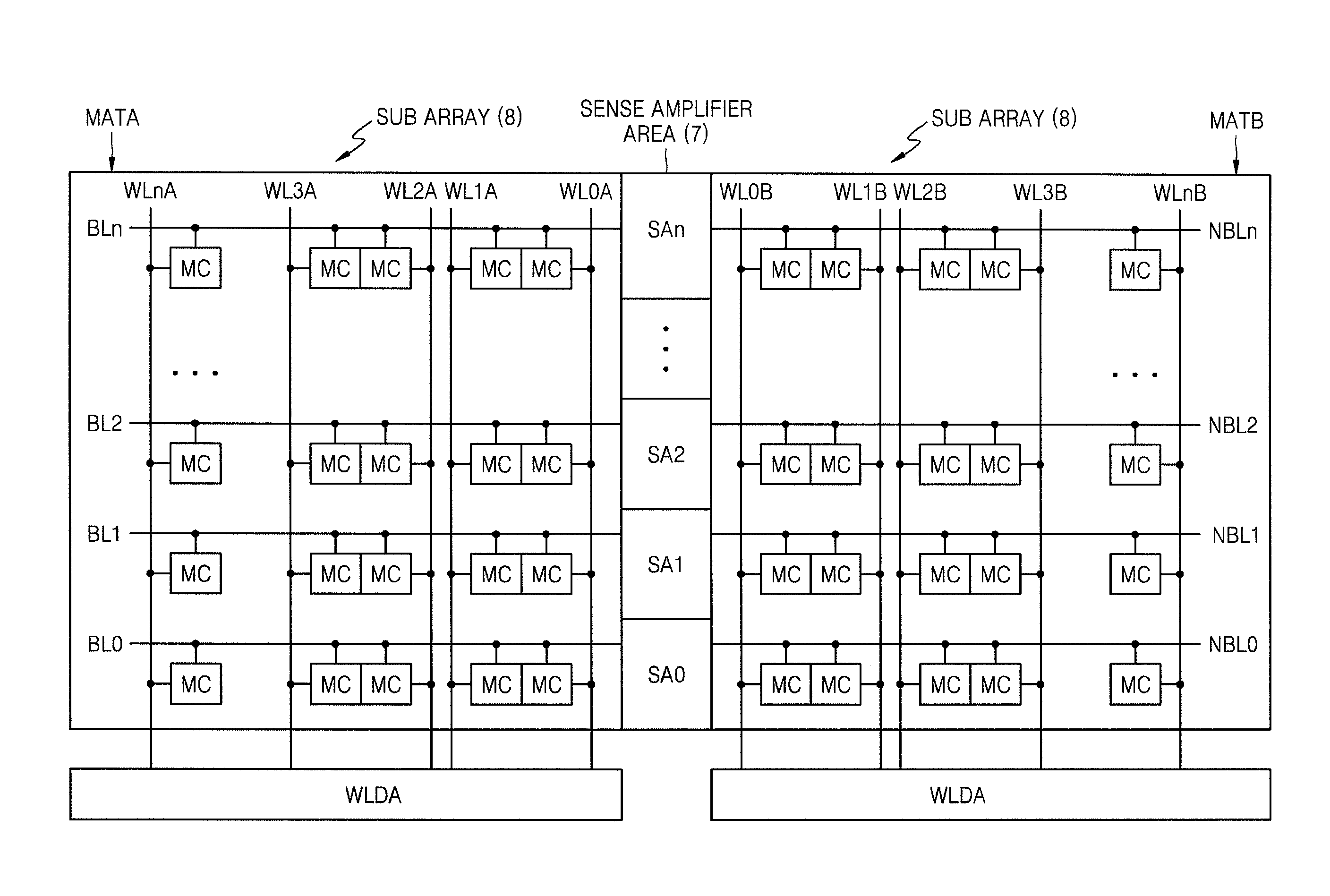
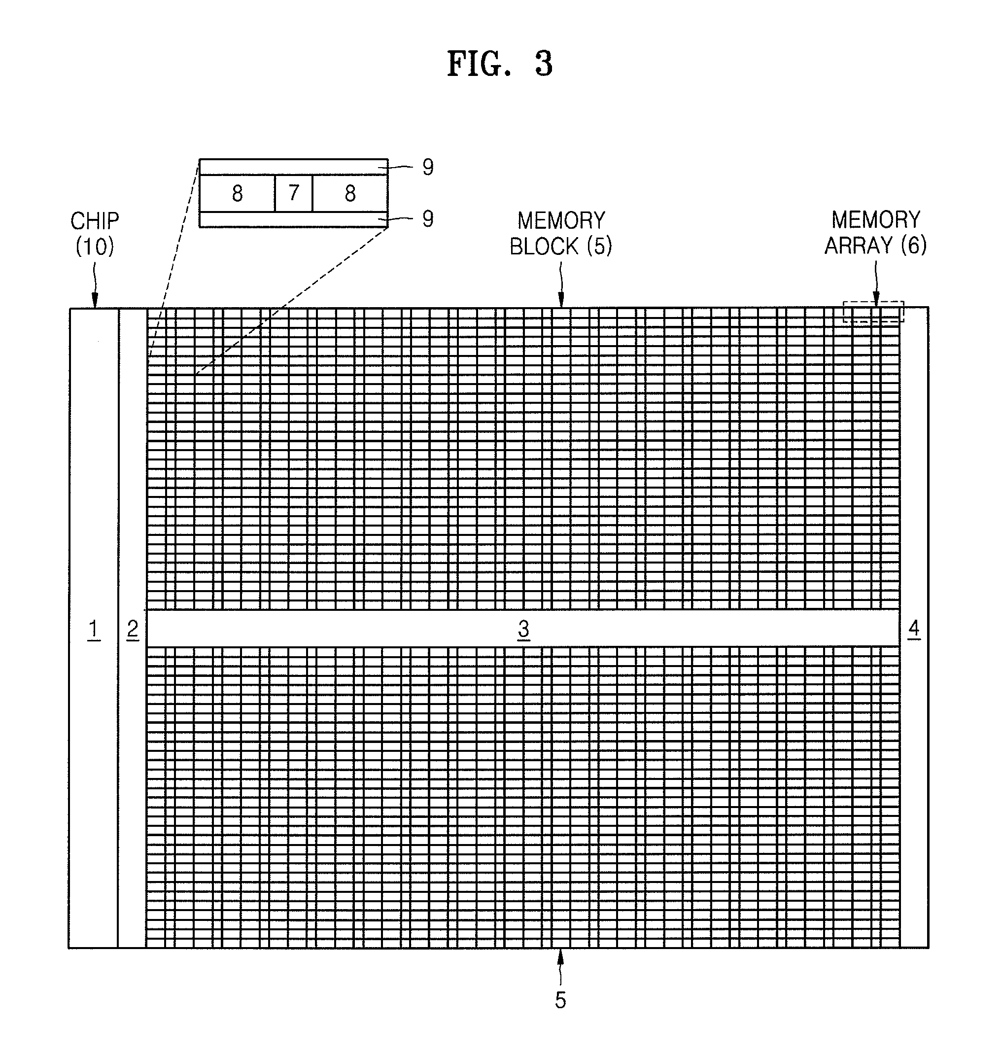
[0040]Among semiconductor memory devices having large storage capacity, low power consumption and fast operational performance, a dynamic random access memory (DRAM) senses and amplifies data read from a memory cell by using a bit line sense amplifier. The bit line sense amplifier does this by developing a voltage difference between a bit line pair, which is caused by a charge-shared between the bit line receiving the data and a capacitor of the memory cell sending the data. Data sensed and amplified by the bit line sense amplifier is transmitted to a data line and is sensed and amplified by a data line sense amplifier to be read out.

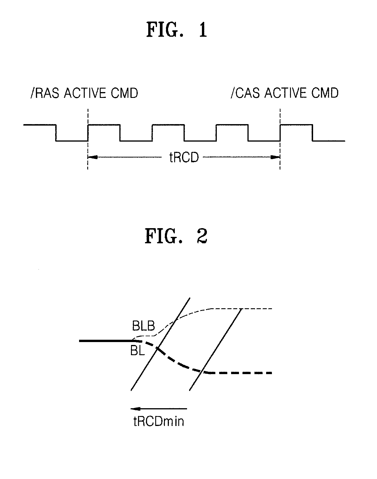
[0041]A row address strode ( / RAS) to column address strobe ( / CAS) delay time (tRCD), which is a parameter that contributes to the high-speed opera...


PUM


Abstract

A semiconductor memory device including: first and second memory cell arrays each including at least one word line, at least three bit lines, and memory cells; and a sense amplifier area disposed between the first and second memory cell arrays and including a sense amplifier circuit for sensing and amplifying data of the memory cells, wherein the at least three bit lines of the first memory cell array and the at least three bit lines of the second memory cell array extend in a first direction and the at least three bit lines of the first and the second memory cell arrays are respectively connected to data lines disposed in a second direction, and wherein a bit line located between two of the at least three bit lines of each of the first and the second memory cell arrays is connected to an outermost data line of the data lines.

Description

CROSS-REFERENCE TO RELATED APPLICATION[0001]This application claims priority under 35 U.S.C. §119 to Korean Patent Application No. 10-2010-0006498, filed on Jan. 25, 2010, in the Korean Intellectual Property Office, the disclosure of which is incorporated by reference herein in its entirety.BACKGROUND[0002]1. Technical Field[0003]The inventive concept relates to a semiconductor memory device, and more particularly, to a semiconductor memory device for reducing bit line coupling noise.[0004]2. Discussion of the Related Art[0005]Semiconductor memory devices having large storage capacity, low power consumption, and fast operational performance are being, and have been, developed. However, as storage capacity increases, so does interference noise between adjacent bit lines of the semiconductor memory devices. Further, in semiconductor memory devices that have low power consumption, an operating voltage used to perform a data access operation, such as a read operation and a write operati...

Claims


Application Information

Patent Timeline
Patent Type & Authority Patents(United States)
IPC IPC(8): G11C5/06
CPCG11C5/063G11C7/02G11C11/4097G11C5/06G11C7/06G11C7/12G11C7/18G11C11/4094
Inventor KIM, SANG-YUNKO, TAI-YOUNG
Owner SAMSUNG ELECTRONICS CO LTD
Why Eureka
Try Eureka