Method for forming pillar type capacitor of semiconductor device

a technology of semiconductor devices and capacitors, which is applied in the direction of capacitors, semiconductor devices, electrical equipment, etc., can solve the problems of difficult use of cylinder-type storage nodes in giga dram products having a fine metal line width, and achieve the effect of reducing contact resistan

Active Publication Date: 2013-06-25
SK HYNIX INC
View PDF11 Cites 30 Cited by
  • Summary
  • Abstract
  • Description
  • Claims
  • Application Information

AI Technical Summary

Benefits of technology

[0011]The pillar type capacitor further comprises: an interlayer insulating film disposed to substantially the same height as the storage node contact; and a metal layer disposed over the upper portion of the interlayer insulating film and the storage node contact and in contact with the bottom electrode, thereby reducing a contact resistance.
[0012]The metal layer is at least one of: Ti and TiSi. The pillar type capacitor where the upper portion of the pillar comprises a storage node oxide pillar. The additional height of the pillar due to the storage node oxide pillar increases electrode area of the pillar type capacitor.
[0018]After forming a storage node contact, the method further comprises forming a metal layer in contact with the bottom electrode and over the upper portion of the storage node contact, thereby minimizing a contact resistance. The metal layer includes Ti or TiSi.
[0026]Before forming a bottom electrode, the method further comprises forming a barrier metal layer over the surface of the pillar, thereby minimizing contact resistance.

Problems solved by technology

However, it is difficult to use the cylinder-type storage node structure in giga DRAM products having a fine metal line width of less than 50 nm because a space where a capacitor can be formed by depositing a dielectric film of about 100 Å and a plate node of about 200 Å is not sufficiently provided in a cell region while securing a space of over 25 nm (250 Å) for insulation between the adjacent storage nodes.

Method used


Image

  • Method for forming pillar type capacitor of semiconductor device
  • Method for forming pillar type capacitor of semiconductor device
  • Method for forming pillar type capacitor of semiconductor device

Examples


Embodiment Construction

[0032]The present invention will be described in detail with reference to the attached drawings.

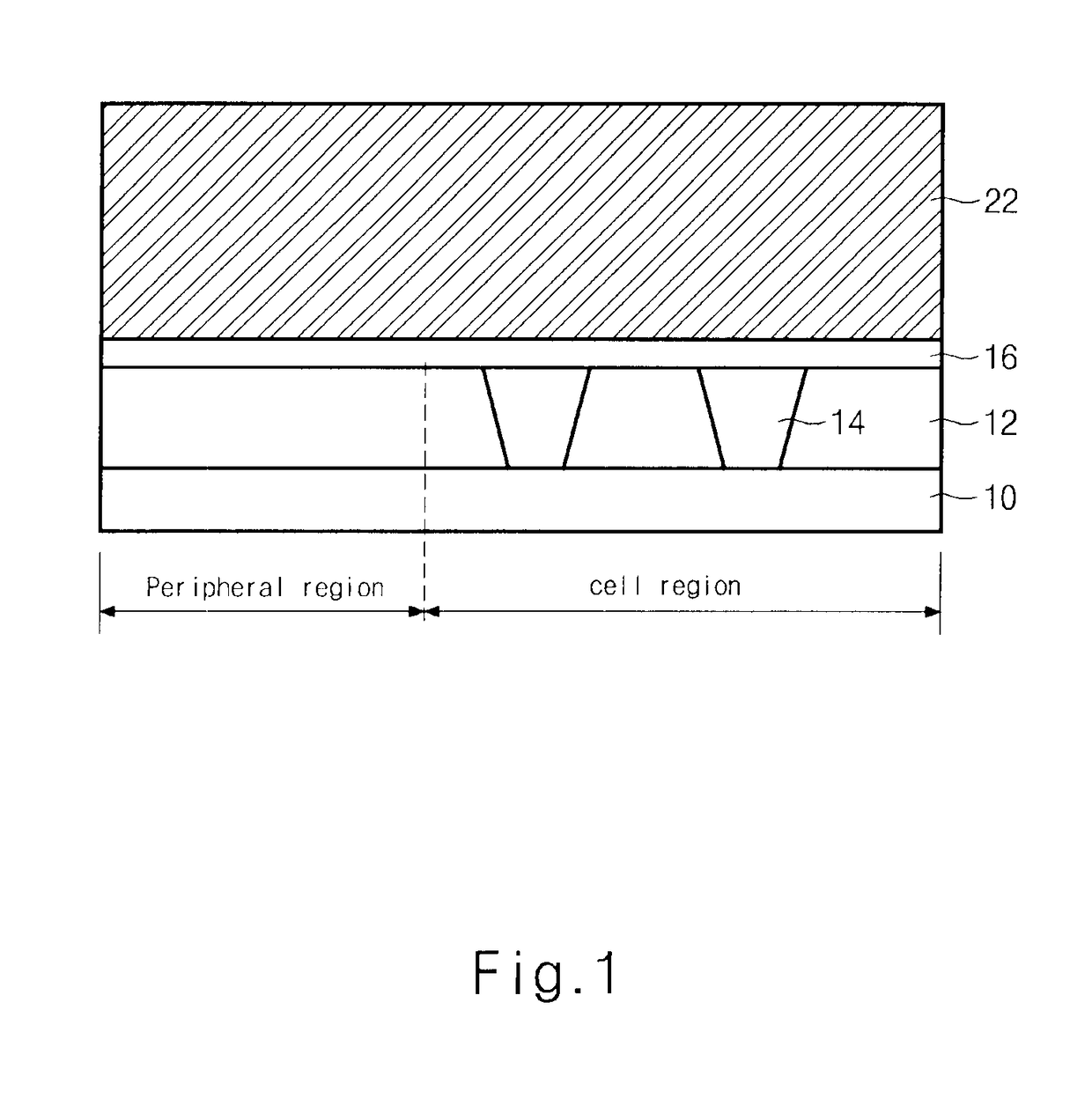
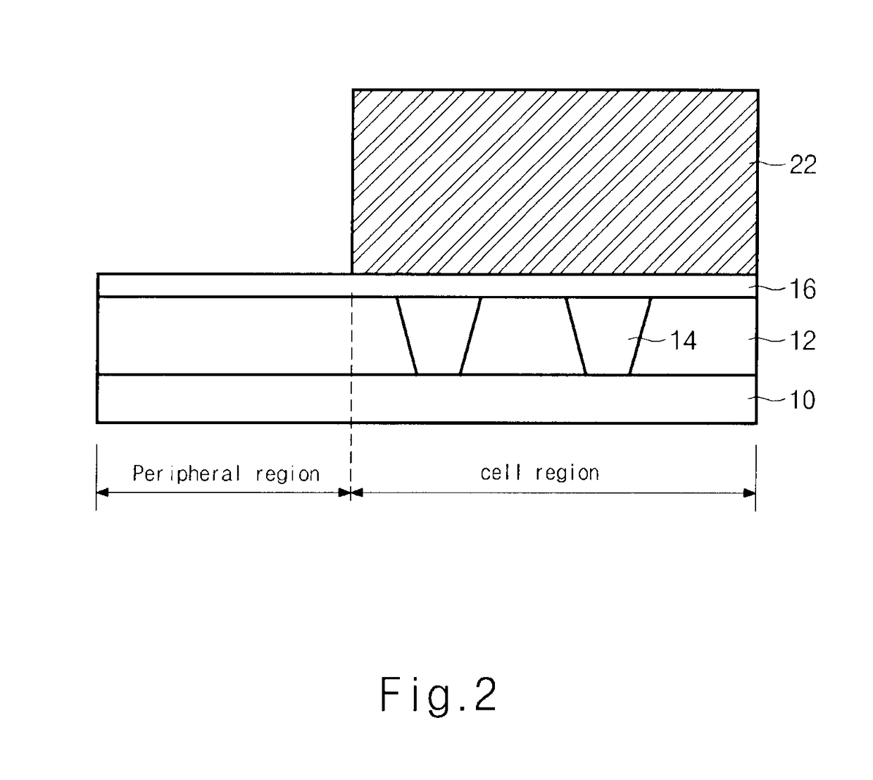
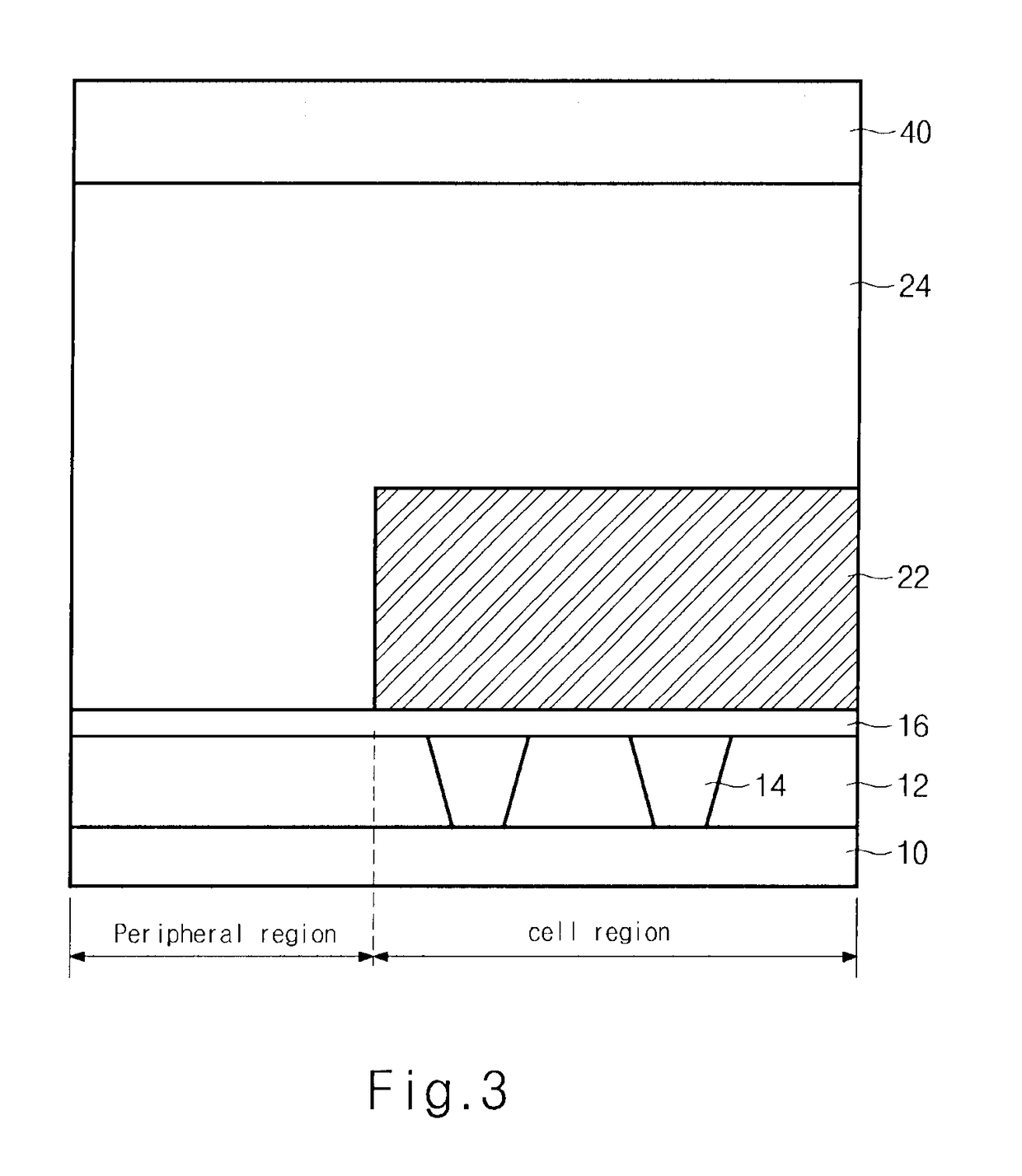
[0033]FIGS. 1 to 9 are diagrams illustrating an exemplary method for forming a pillar type capacitor of a semiconductor device. FIGS. 1-4, 6a, 7-9 are cross-sectional views. FIG. 6b is a perspective view of FIG. 6a. FIGS. 5a and 5b are plane views.

[0034]Referring to FIG. 1, an interlayer insulating film 12, which may comprise, for example, a dielectric material, is formed on a semiconductor substrate 10 including a cell region and a peripheral region. The interlayer insulating film 12 includes an oxide film. A gate or is a bit line is formed in the lower portion of the interlayer insulating film 12.

[0035]After a mask pattern such as a photoresist film is formed on the interlayer insulating film 12 of the cell region, the interlayer insulating film 12 is etched with the mask pattern as a mask to form a storage node contact hole that exposes the semiconductor substrate or a landing plug. A ...


PUM


Abstract

An embodiment of the invention includes a pillar type capacitor where a pillar is formed over an upper portion of a storage node contact. A bottom electrode is formed over sidewalls of the pillar, and a dielectric film is formed over pillar and the bottom electrode. A top electrode is then formed over the upper portion of the dielectric film.

Description

CROSS-REFERENCE TO RELATED APPLICATION[0001]The priority of Korean patent application No. 10-2010-0070128 filed on Jul. 20, 2010, the disclosure of which is hereby incorporated in its entirety by reference, is claimed.BACKGROUND OF THE INVENTION[0002]1. Field of the Invention[0003]An embodiment of the present invention generally relates semiconductor devices, and more specifically to a pillar type capacitor of a semiconductor device and a method for forming the same.[0004]2. Description of the Related Art[0005]Due to rapid development of the process technology of small-sized semiconductors, high-integration of memory products has is been accelerated to reduce the unit cell area and lower the operating voltage. However, the charging capacity required in the operation of memory devices has been continuously required to be over 25 fF / cell in order to prevent generation of soft errors and shortening of the refresh time.[0006]In order to secure the charging capacity required in the next ...

Claims


Application Information

Patent Timeline
Patent Type & Authority Patents(United States)
IPC IPC(8): H01L21/8242
CPCH01L27/10852H01L27/10855H01L27/10894H01L28/90H10B12/033H10B12/0335H10B12/09
Inventor CHO, HO JINPARK, CHEOL HWANLEE, DONG KYUN
Owner SK HYNIX INC
Why Eureka
Try Eureka