Method and apparatus for electroplating

a technology of electroplating and method, applied in the direction of electrochemical machining apparatus, metal-working apparatus, metallic material coating process, etc., can solve the problems of extreme terminal effect situation, non-uniform thickness distribution of plating, and significant limitations of approaches to physical properties of materials and processes, so as to improve plating uniformity

Active Publication Date: 2013-07-02
NOVELLUS SYSTEMS
View PDF143 Cites 32 Cited by
  • Summary
  • Abstract
  • Description
  • Claims
  • Application Information

AI Technical Summary

Benefits of technology

The invention provides an electroplating apparatus and method using an ionically resistive element with electrolyte-permeable pores or holes to improve plating uniformity on thin resistive seed layers. An auxiliary cathode is used to divert or remove current from the anode that would otherwise pass to the edge region of the wafer. The ionically resistive element acts as a virtual anode, resulting in a uniform current density in the proximity of the wafer cathode. This leads to improved plating uniformity.

Problems solved by technology

These thin films, some having inherently large specific resistivities, present the engineer with an extreme terminal effect situation.
Without appropriate means of resistance and voltage compensation, this large edge-to-center voltage drop could lead to an extremely non-uniform plating thickness distribution, primarily characterized by thicker plating at the wafer edge.
These approaches have significant limitations related to the physical properties of the materials and the processes.
Also, because the conductivity of a plating bath is tied to its ionic concentration and pH, decreasing the conductivity directly and negatively impacts the rate of plating and morphology of the plated material.
The plating electrolyte contained within the pores of the HRVA allows ionic current to pass though the disk, but at a significant voltage drop compared to the system as a whole.

Method used


Image

  • Method and apparatus for electroplating
  • Method and apparatus for electroplating
  • Method and apparatus for electroplating

Examples


Embodiment Construction

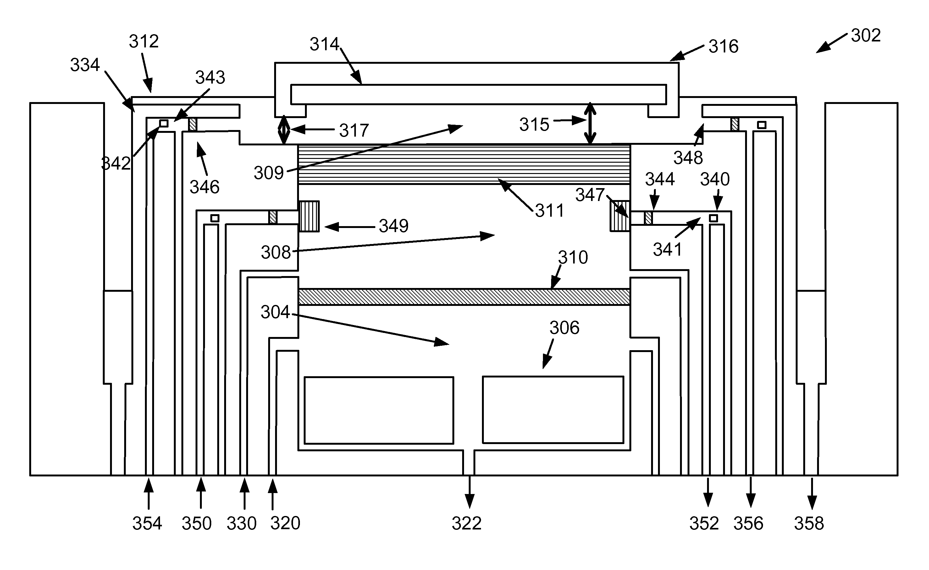
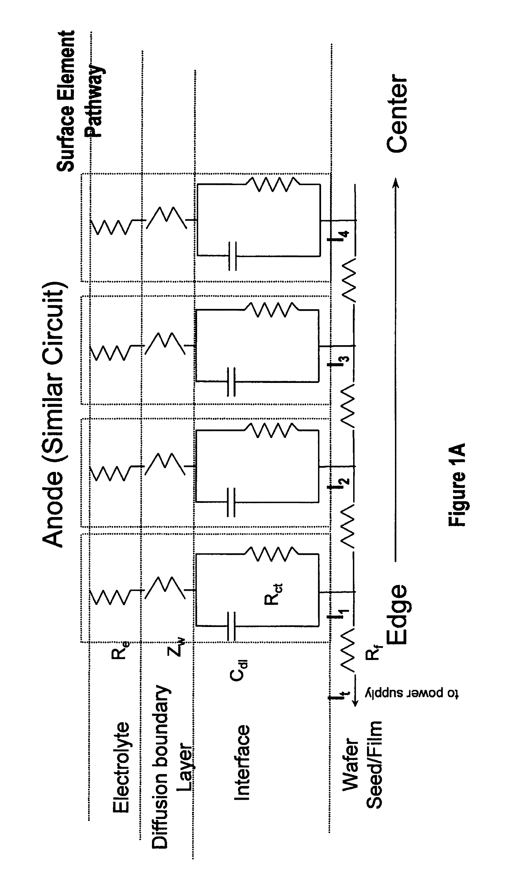
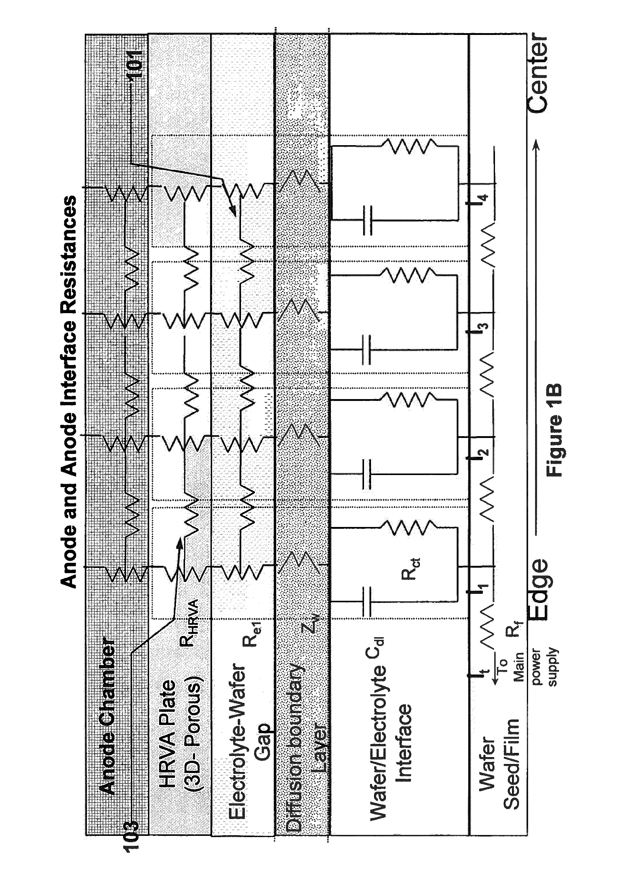
[0031]Advanced technologies call for the electroplating of metals onto wafers with sheet resistances of 10 ohm per square and higher (even 20 ohms per square or 40 ohms per square or higher). This requires ever more aggressive techniques (i.e., techniques other than only the use of a HRVA alone or a thief electrode alone) to compensate for the terminal effect. During plating, the thickness of metal and the sheet resistance can drop several orders of magnitude in a short time, and so methods and apparatus capable of plating uniformly on the wafer throughout a process where there may be a rapidly initially varying and later a relatively constant sheet resistance are required. Embodiments of the present invention address the challenges presented by such high resistance seed layers, the rapid dynamic variance in the seed electrical parameters, and the extreme terminal effect they present.

[0032]Embodiments of the present invention pertain to methods and apparatuses for electroplating a s...


PUM

PropertyMeasurementUnit
edge voltageaaaaaaaaaa
voltage dropaaaaaaaaaa

Abstract

An apparatus for electroplating a layer of metal onto the surface of a wafer includes an ionically resistive ionically permeable element located in close proximity of the wafer and an auxiliary cathode located between the anode and the ionically resistive ionically permeable element. The ionically resistive ionically permeable element serves to modulate ionic current at the wafer surface. The auxiliary cathode is configured to shape the current distribution from the anode. The provided configuration effectively redistributes ionic current in the plating system allowing plating of uniform metal layers and mitigating the terminal effect.

Description

CROSS-REFERENCE TO RELATED APPLICATIONS[0001]This application is a continuation-in part of U.S. application Ser. No. 12 / 291,356, filed Nov. 7, 2008, now issued as U.S. Pat. No. 8,308,931, naming Reid et al. as inventors, which is herein incorporated by reference in its entirety and for all purposes.BACKGROUND OF THE INVENTION[0002]The transition from aluminum to copper in integrated circuit (IC) fabrication required a change in process “architecture” (to damascene and dual-damascene) as well as a whole new set of process technologies. One process step used in producing copper damascene circuits is the formation of a “seed-” or “strike-” layer, which is then used as a base layer onto which copper is electroplated (electrofill). The seed layer carries the electrical plating current from the edge region of the wafer (where electrical contact is made) to all trench and via structures located across the wafer surface. The seed film is typically a thin conductive copper layer. It is separ...

Claims


Application Information

Patent Timeline
Patent Type & Authority Patents(United States)
IPC IPC(8): C25D17/12C25D21/12
CPCC23C18/1601C25D17/002C25D17/007C25D17/008C25F3/30H01L21/2885H01L21/32115H01L21/32125C25D17/12C25D21/12C25D17/001C25D5/02C25D21/14H01L21/6715H01L21/76873C25D17/02C25D17/08C25D17/10H01L21/28
Inventor MAYER, STEVENFENG, JINGBINHE, ZHIANREID, JONATHANVARADARAJAN, SESHASAYEE
Owner NOVELLUS SYSTEMS
Why Eureka
Try Eureka