Three axis magnetic sensor device and method

a magnetic sensor and three-axis technology, applied in galvano-magnetic hall-effect devices, three-component magnetometers, instruments, etc., can solve the problems of cost, and difficulty in magnetic sensor and mem development, and achieve the effect of high device yield in dies and convenient us

Active Publication Date: 2013-07-16
MOVELLA INC
View PDF59 Cites 34 Cited by
  • Summary
  • Abstract
  • Description
  • Claims
  • Application Information

AI Technical Summary

Benefits of technology

[0009]Many benefits are achieved by way of embodiments the present invention over conventional techniques. For example, embodiments of the present technique provide an easy to use process to integrate a three-axis magnetic field sensor on a single die. In some embodiments, the method provides higher device yields in dies per wafer with the integrated approach. Additionally, the method provides a process and system that are compatible with conventional semiconductor and MEMS process technologies without substantial modifications to conventional equipment and processes. Preferably, the invention provides for an improved magnetic field sensor or magne

Problems solved by technology

Although highly successful, ICs and in particular magnetic field sensors and MEMS still have limitations.
Similar to IC development, magnetic sensor and MEMS development, which focuses on increasing performance, reducing size, and decreas

Method used


Image

  • Three axis magnetic sensor device and method
  • Three axis magnetic sensor device and method
  • Three axis magnetic sensor device and method

Examples


Embodiment Construction

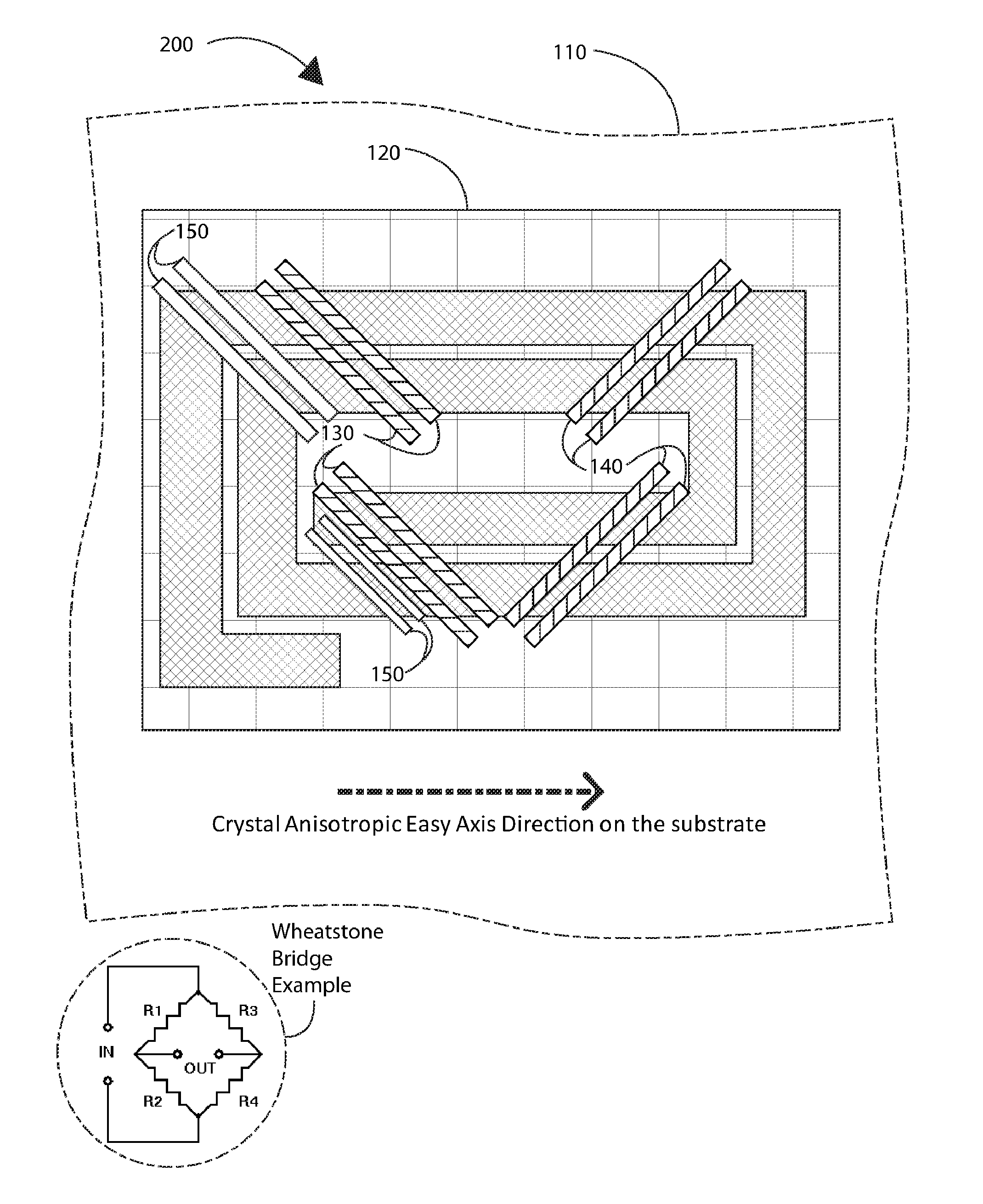
[0022]According to embodiments of the present invention, techniques related generally to integrated devices and systems are provided. In particular, embodiments of the present invention provide methods and structures for a three-axis magnetic field sensing device. More specifically, embodiments of the present invention provide methods for forming at least one a first, second, and third magnetic field sensor element overlying a substrate member with field concentrator(s) and operably coupled to an integrated circuit (IC) layer. Merely by way of example, the magnetic field sensor elements can include ordinary magneto-resistive (OMR) device(s), anisotropic magneto-resistive (AMR) devices, giant magneto-resistive (GMR) device(s), tunnel-junction magneto-resistive (TMR), or others. Additionally, other applications include at least a sensor application or magnetic field sensing applications, system applications, among others.

[0023]FIG. 1 is a simplified top diagram of a device for sensing...


PUM


Abstract

A method and structure for a three-axis magnetic field sensing device is provided. The device includes a substrate, an IC layer, and preferably three magnetic field sensors coupled to the IC layer. A nickel-iron magnetic field concentrator is also provided.

Description

BACKGROUND OF THE INVENTION[0001]This invention relates generally to integrated devices. More specifically, the invention provides an integrated transducer apparatus that can be used in combination with other Micro-electromechanical systems (MEMS) devices, but can have other uses as well. For example, the MEMS devices can provide an accelerometer, an angular rate sensor, a magnetic field sensor, a pressure sensor, a microphone, a humidity sensor, a temperature sensor, a chemical sensor, a biosensor, an inertial sensor, and others.[0002]Research and development in integrated microelectronics have continued to produce progress in CMOS and MEMS technology. CMOS technology has become the predominant fabrication technology for integrated circuits (ICs). In layman's terms, the ICs are the “brains” of an integrated device and provide decision-making capabilities, while MEMS are the “eyes” and “arms” and provide the ability to sense and control the environment. Some examples of the widespre...

Claims


Application Information

Patent Timeline
IPC IPC(8): H01L29/82G11C11/02
CPCH01L27/22G01R33/0206G01R33/093H01L43/08H01L43/12G01R33/0286H10B61/00H10N59/00H10N50/01H10N50/10
Inventor WAN, HONGYANG, XIAO "CHARLES"
Owner MOVELLA INC
Why Eureka
Try Eureka