Reverse-conducting insulated gate bipolar transistor

a bipolar transistor and insulated gate technology, applied in the direction of electrical equipment, semiconductor devices, wellbore/well accessories, etc., can solve the problems of difficult latching up condition, etc., and achieve the effect of reducing the cost of the chip

Inactive Publication Date: 2013-08-06
FUJI ELECTRIC CO LTD
View PDF18 Cites 16 Cited by
  • Summary
  • Abstract
  • Description
  • Claims
  • Application Information

AI Technical Summary

Benefits of technology

[0010]In view of the above-described issues, the present invention provides a reverse-conducting insulated gate bipolar transistor in which an IGBT region and an FWD region are integrated into a single body operating in one and the same active region and a chip cost is reduced by at least 30%.
[0016]According to the present invention, a reverse-conducting insulated gate bipolar transistor is provided in which an IGBT region and an FWD region are integrated into a single body operating in one and the same active region and a chip cost is reduced by at least 30%.

Problems solved by technology

Since a large magnitude of electron current is necessary to attain a voltage drop value around the junction surface required by the latching up, a “snap-back” occurs in the I-V waveform in the ON state causing a difficult condition for turning the IGBT region ON (or a difficult condition for latching up).
Nevertheless, the latching up is not easy to achieve and a snap-back phenomenon is apt to occur caused by the existence of an n+ cathode region in a p+ collector region side, in comparison with an ordinary IGBT that is not a reverse-conducting type or a collector-shorted type.
However, the n+ FS region has a high impurity concentration and a low resistivity.
However, in a method to integrate an IGBT region and an FWD region monolithically into one chip, an integrated structure obtained by simply dividing the major active region of a semiconductor substrate into two regions as disclosed in Japanese Unexamined Patent Application Publication No. 2004-363328 is absolutely impossible to provide a cost reduction effect of 30%.
Therefore, the RC-IGBT cannot benefit from the integration of the IGBT region and the FWD region into a single chip by means of the method disclosed in Japanese Unexamined Patent Application Publication No. 2007-184486, and the chip cost cannot be reduced yet.

Method used


Image

  • Reverse-conducting insulated gate bipolar transistor
  • Reverse-conducting insulated gate bipolar transistor
  • Reverse-conducting insulated gate bipolar transistor

Examples


embodiment 1

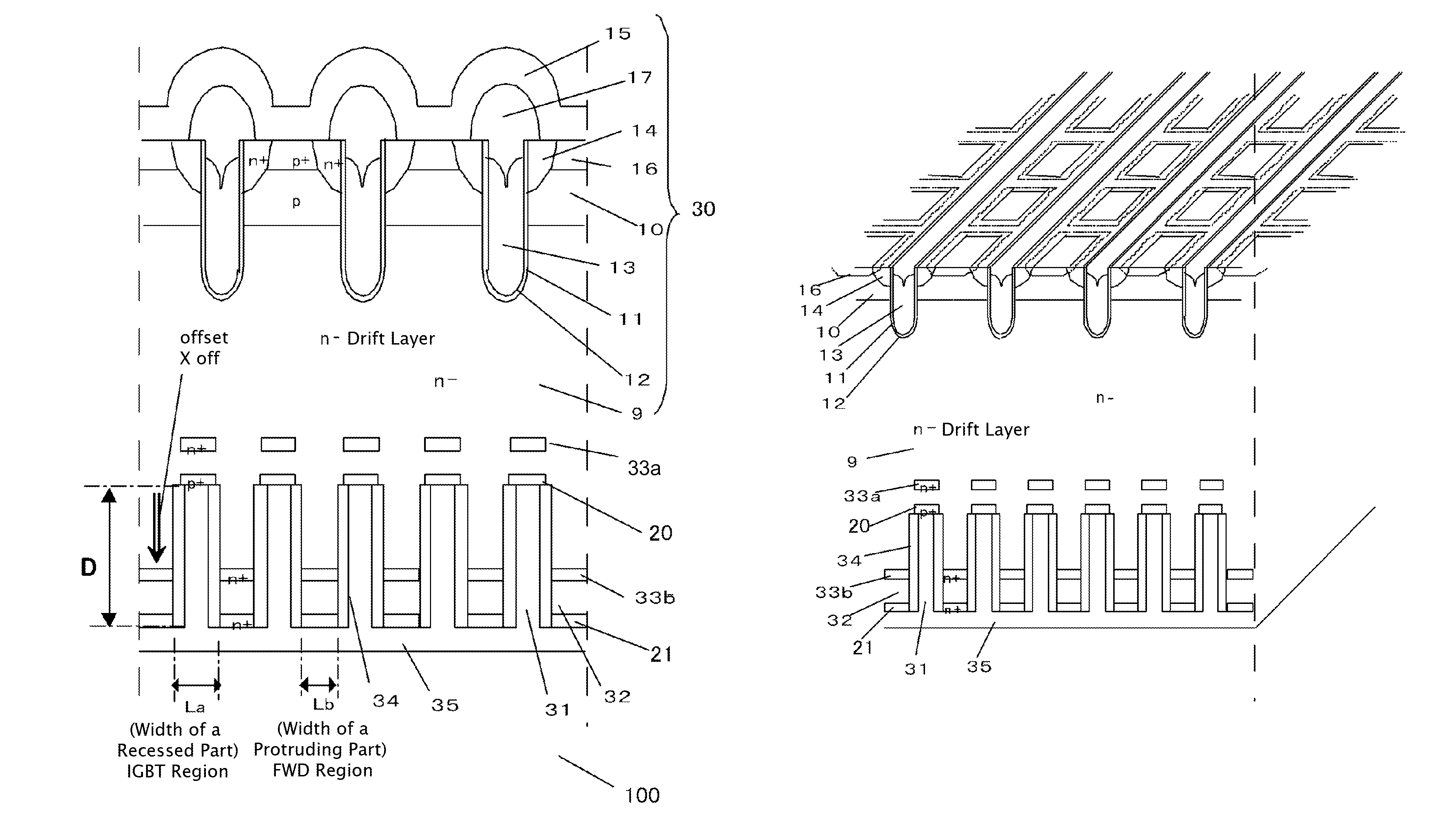
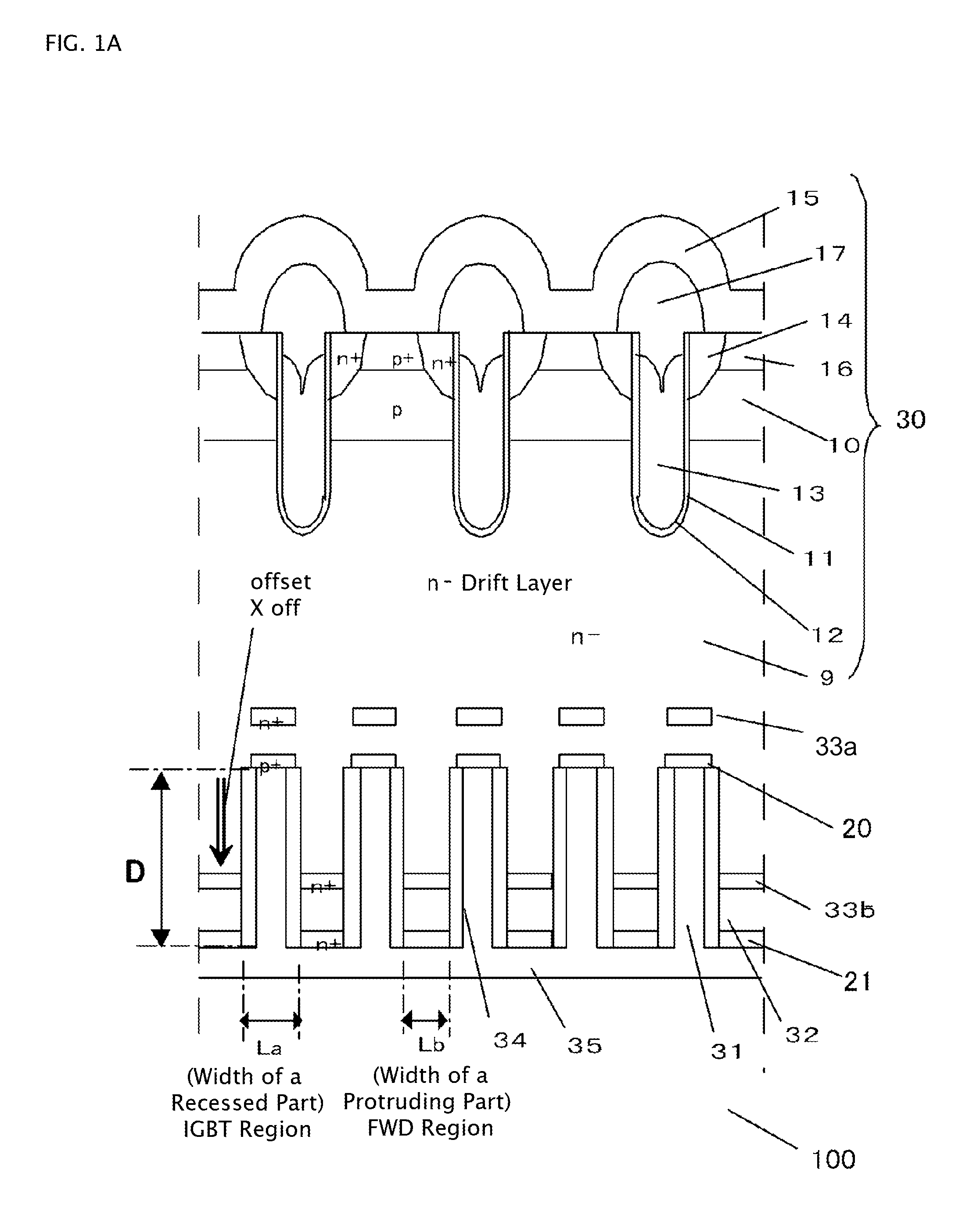
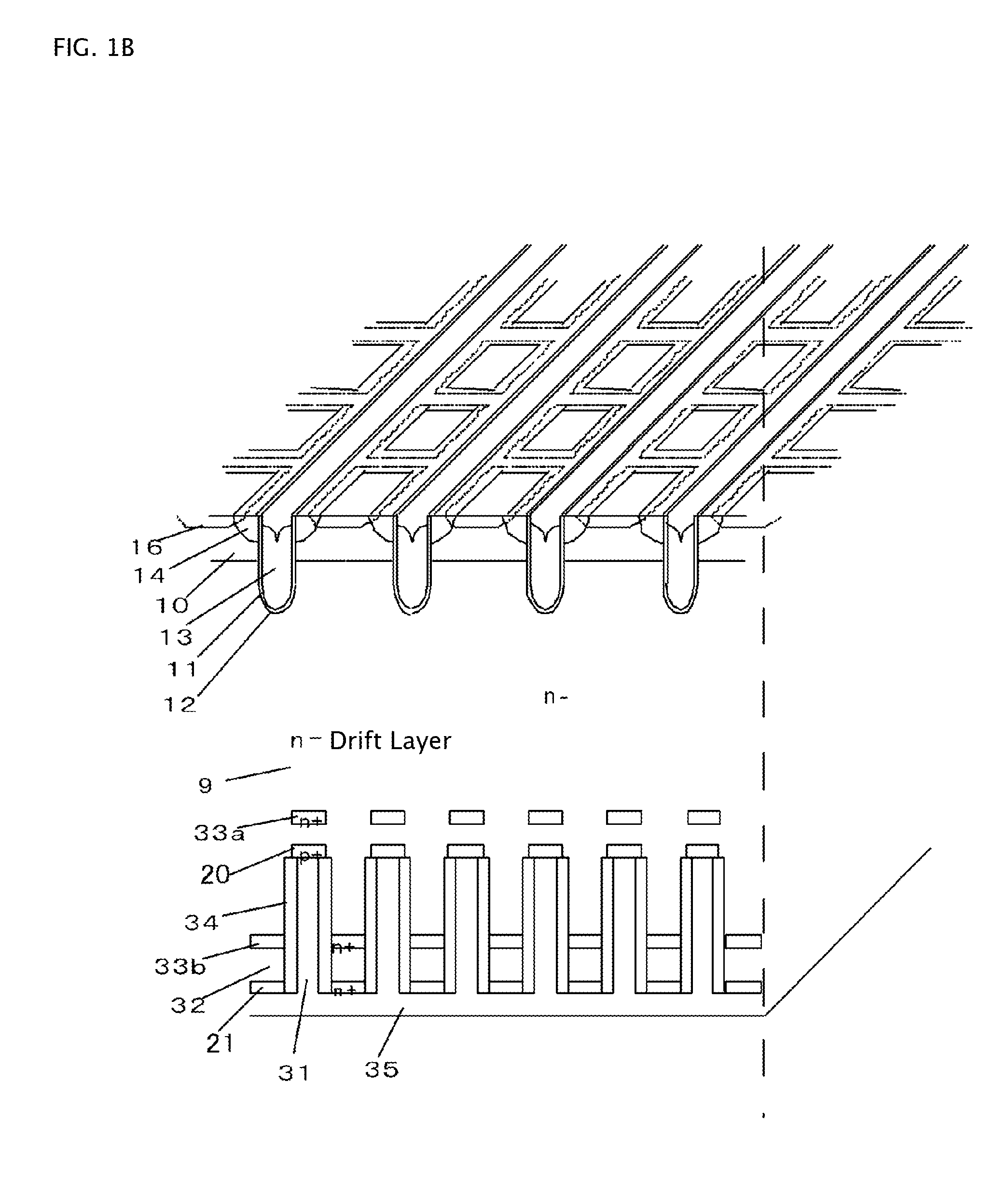
[0025]FIGS. 1(a) and 1(b) show an essential part of the RC-IGBT of Embodiment 1 according to the present invention, in which FIG. 1(a) is a sectional view and FIG. 1(b) is a perspective view. In FIG. 1(b), interlayer dielectric film 17 and emitter electrode 15 both depicted in FIG. 1(a) are omitted. The following describes in detail a structure and a manufacturing method of the RC-IGBT according to the invention.

[0026]In conventional RC-IGBTs, an FWD is incorporated into an ordinary FS-IGBT in an anti-parallel connection to the IGBT on a single semiconductor substrate. In an RC-IGBT of a conventional construction in general, the anti-parallel connected FWD comprises an anode layer that is a p base layer contained in a MOS gate structure in the front surface side of a semiconductor substrate and a cathode layer of n+ cathode region that is formed by replacing a part of an ordinary p+ collector region in the rear surface side.

[0027]In the RC-IGBT 100 of Embodiment 1 according to the p...


PUM


Abstract

Reverse-conducting insulated gate bipolar transistor in which IGBT region and FWD region are integrated into a single body in a semiconductor substrate with a common active region is disclosed. MOS gate structure is on a first major surface side. Rear surface side structure is in a second major surface side of the semiconductor substrate and includes a plurality of recessed parts vertical to the second major surface, which are repeated periodically along the second major surface. A plurality of protruding parts are interposed between the recessed parts. Rear surface side structure includes p type collector region on a bottom surface of the recessed part, n type first field stop region at a position deeper than the collector region, n type cathode region on the top surface of the protruding part, and n type second field stop region in the protruding part at a position deeper than the cathode region.

Description

BACKGROUND OF THE INVENTION[0001]A. Field of the Invention[0002]The present invention relates to a reverse-conducting insulated gate bipolar transistor (hereinafter also abbreviated to an RC-IGBT) that is provided with an insulated gate bipolar transistor (hereinafter also abbreviated to an IGBT) and a diode that is anti-parallel-connected to the IGBT, both disposed on one and the same semiconductor substrate.[0003]B. Description of the Related Art[0004]Performance improvement in power semiconductor devices is in progress in insulated gate bipolar transistors (IGBTs) and free-wheeling diodes (FWDs) for withstand voltage class of 600 V, 1,200 V, and 1,700 V. Those power semiconductor devices are used in high speed, high efficiency and power saving power conversion equipment including converters and inverters, and are indispensable for controlling rotating motors and servo motors. The power control apparatuses confront growing requests of the market for low losses (power saving), high...

Claims


Application Information

Patent Timeline
Patent Type & Authority Patents(United States)
IPC IPC(8): E21B49/00
CPCH01L29/739H01L29/7397H01L29/0834H01L29/0696H01L29/66348
Inventor NEMOTO, MICHIOYOSHIDA, SOUICHI
Owner FUJI ELECTRIC CO LTD
Why Eureka
Try Eureka