Method of forming a compliant bipolar micro device transfer head with silicon electrodes

a technology of silicon electrodes and transfer heads, applied in the field of micro devices, can solve problems such as integration and packaging

Active Publication Date: 2013-10-29
APPLE INC
View PDF74 Cites 46 Cited by
  • Summary
  • Abstract
  • Description
  • Claims
  • Application Information

AI Technical Summary

Benefits of technology

[0018]In an embodiment, the dielectric layer is etched to expose each of the mesa structures simultaneously with etching through the buried oxide layer to expose the portion of the base substrate. A second dielectric layer can then be formed over each of the mesa structures. In an embodiment, this may be accomplished by blanket deposition of the second dielectric layer followed by removal of a portion of the second dielectric layer. In some embodiments, blanket deposition may be accomplished by atomic layer deposition. In an embodiment, the dielectric layer may be additionally etched to expose a portion of the first and second silicon interconnects, followed by etching a first topside via opening through the exposed portion of the first silicon interconnect and the buried oxide layer, etching a second topside via opening through the exposed portion of the second silicon interconnect and the buried oxide layer, and forming a patterned conductive layer within the first and second topside via openings to make electrical contact with the silicon interconnect and second silicon interconnect. The second dielectric layer formed over each of the mesa structures and the conductive layer formed within the first and second topside via openings may also be used as an etching mask when etching the one or more cavities.

Problems solved by technology

Integration and packaging issues are one of the main obstacles for the commercialization of micro devices such as radio frequency (RF) microelectromechanical systems (MEMS) microswitches, light-emitting diode (LED) display systems, and MEMS or quartz-based oscillators.

Method used


Image

  • Method of forming a compliant bipolar micro device transfer head with silicon electrodes
  • Method of forming a compliant bipolar micro device transfer head with silicon electrodes
  • Method of forming a compliant bipolar micro device transfer head with silicon electrodes

Examples


Embodiment Construction

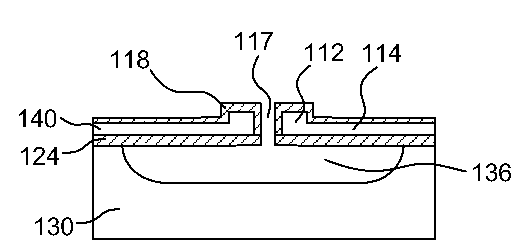
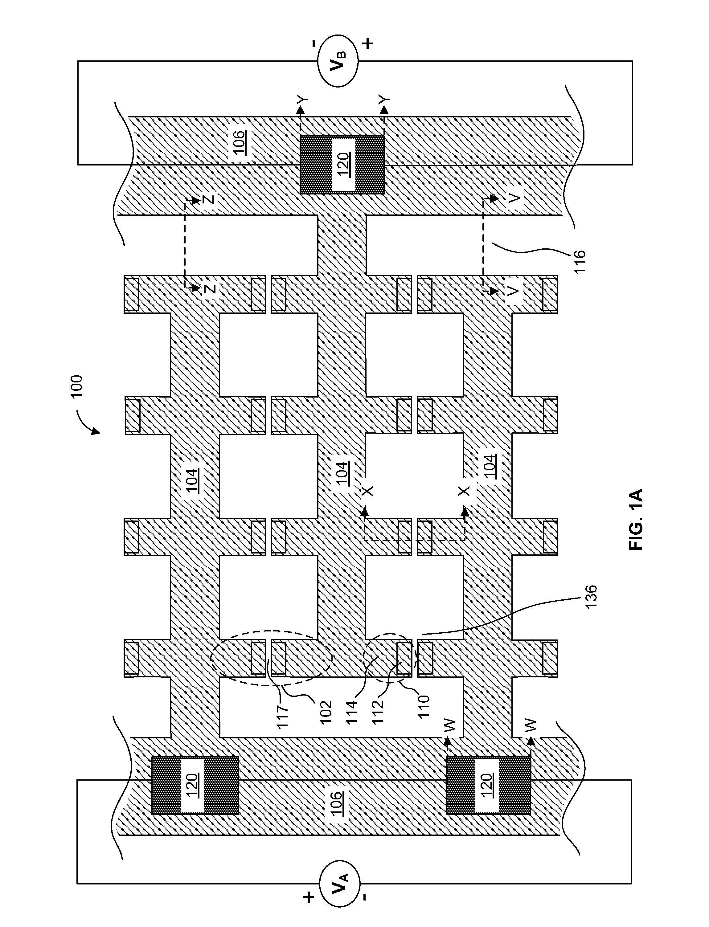
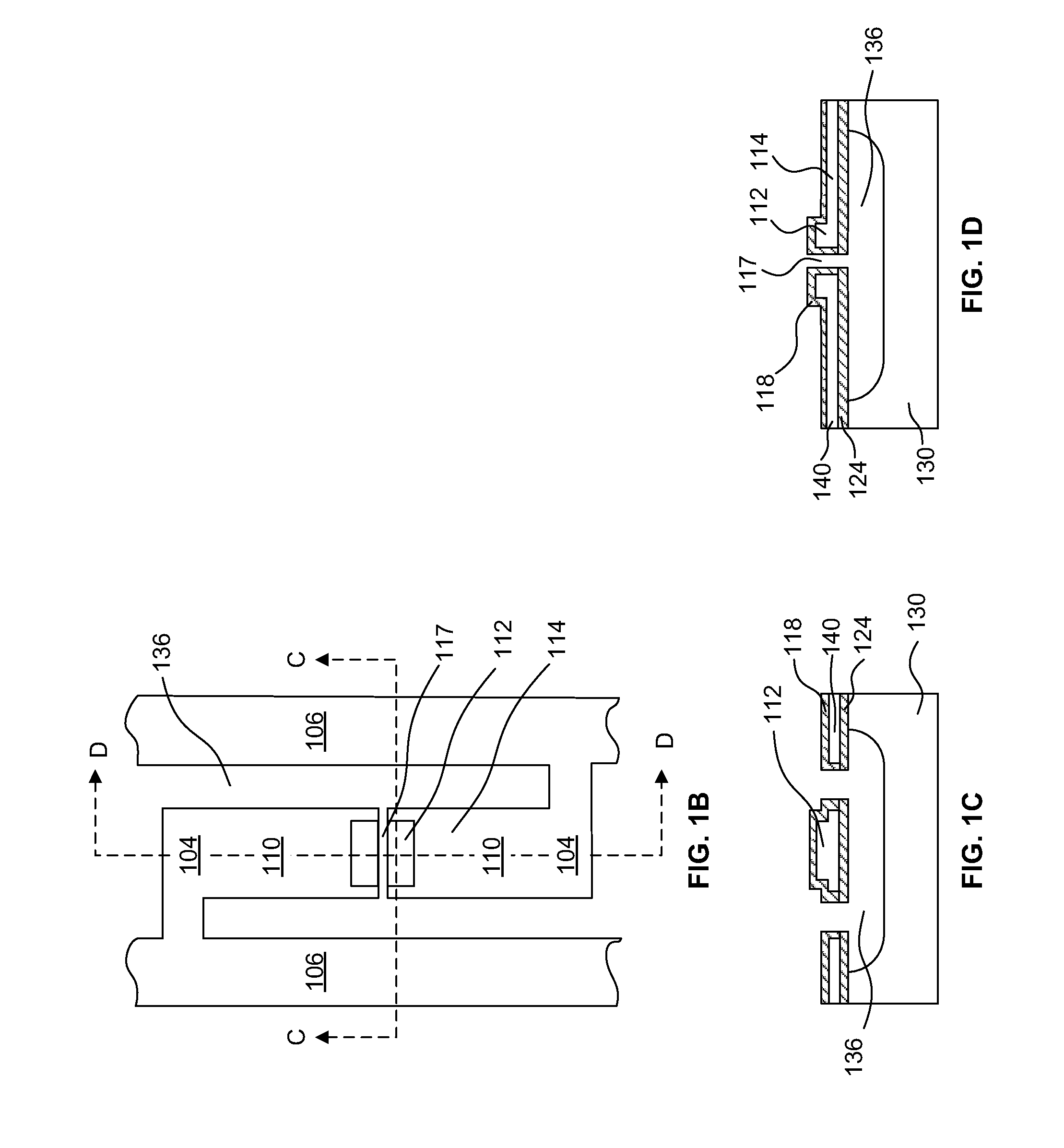
[0045]Embodiments of the present invention describe a compliant bipolar micro device transfer head and head array, and method of transferring a micro device and an array of micro devices to a receiving substrate. For example, the compliant bipolar micro device transfer head and head array may be used to transfer micro devices such as, but not limited to, diodes, LEDs, transistors, ICs, and MEMS from a carrier substrate to a receiving substrate such as, but is not limited to, a display substrate, a lighting substrate, a substrate with functional devices such as transistors or integrated circuits (ICs), or a substrate with metal redistribution lines.

[0046]In various embodiments, description is made with reference to figures. However, certain embodiments may be practiced without one or more of these specific details, or in combination with other known methods and configurations. In the following description, numerous specific details are set forth, such as specific configurations, dime...


PUM


Abstract

A compliant bipolar micro device transfer head array and method of forming a compliant bipolar micro device transfer array from an SOI substrate are described. In an embodiment, a compliant bipolar micro device transfer head array includes a base substrate and a patterned silicon layer over the base substrate. The patterned silicon layer may include first and second silicon interconnects, and first and second arrays of silicon electrodes electrically connected with the first and second silicon interconnects and deflectable into one or more cavities between the base substrate and the silicon electrodes.

Description

BACKGROUND[0001]1. Field[0002]The present invention relates to micro devices. More particularly embodiments of the present invention relate to a compliant bipolar micro device transfer head and a method of transferring one or more micro devices to a receiving substrate.[0003]2. Background Information[0004]Integration and packaging issues are one of the main obstacles for the commercialization of micro devices such as radio frequency (RF) microelectromechanical systems (MEMS) microswitches, light-emitting diode (LED) display systems, and MEMS or quartz-based oscillators.[0005]Traditional technologies for transferring of devices include transfer by wafer bonding from a transfer wafer to a receiving wafer. One such implementation is “direct printing” involving one bonding step of an array of devices from a transfer wafer to a receiving wafer, followed by removal of the transfer wafer. Another such implementation is “transfer printing” involving two bonding / de-bonding steps. In transfer...

Claims


Application Information

Patent Timeline
Patent Type & Authority Patents(United States)
IPC IPC(8): H01L21/82
CPCB81C99/002H01L21/266H01L29/0692H01L29/0619H01L29/06B32B38/18Y10T156/17H01L29/872H01L29/7813H01L29/7806H01L29/66348H01L29/8725H01L29/407H01L29/0696H01L29/66143H01L24/75H01L2224/7598H01L21/6833H01L2924/1461H02N13/00H01L21/3083H01L21/76264
Inventor GOLDA, DARIUSZBIBL, ANDREAS
Owner APPLE INC
Why Eureka
Try Eureka