All-silicon MEMS device structure and manufacture method thereof

A device and structural layer technology, applied in the field of all-silicon MEMS device structure and its manufacturing, can solve the problems of back-splash damage on the back of the suspended structure, increased processing cost, and affect device performance, etc., and achieves convenient standard process, good air tightness, A simple way to achieve the effect

Active Publication Date: 2015-02-18
EAST CHINA INST OF OPTOELECTRONICS INTEGRATEDDEVICE
View PDF6 Cites 18 Cited by
  • Summary
  • Abstract
  • Description
  • Claims
  • Application Information

AI Technical Summary

Problems solved by technology

The MEMS process method based on silicon-glass bonding is simple, but the residual stress after bonding the silicon wafer and glass affects the performance of the device; in the processing method based on the silicon-silicon bonding process, the silicon on the top layer of the substrate SOI silicon wafer is used as the interconnection line. The bottom surface needs to be covered by a s

Method used


Image

  • All-silicon MEMS device structure and manufacture method thereof
  • All-silicon MEMS device structure and manufacture method thereof
  • All-silicon MEMS device structure and manufacture method thereof

Examples


Embodiment Construction

[0025] The present invention will be further described below in conjunction with the accompanying drawings.

[0026] 1. MEMS device structure:

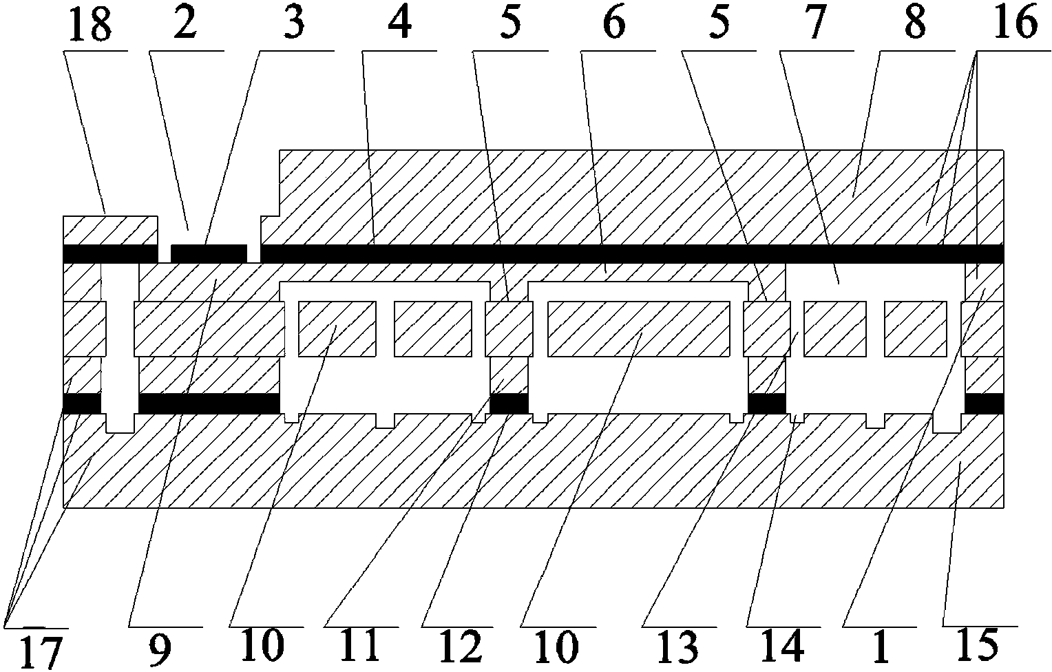
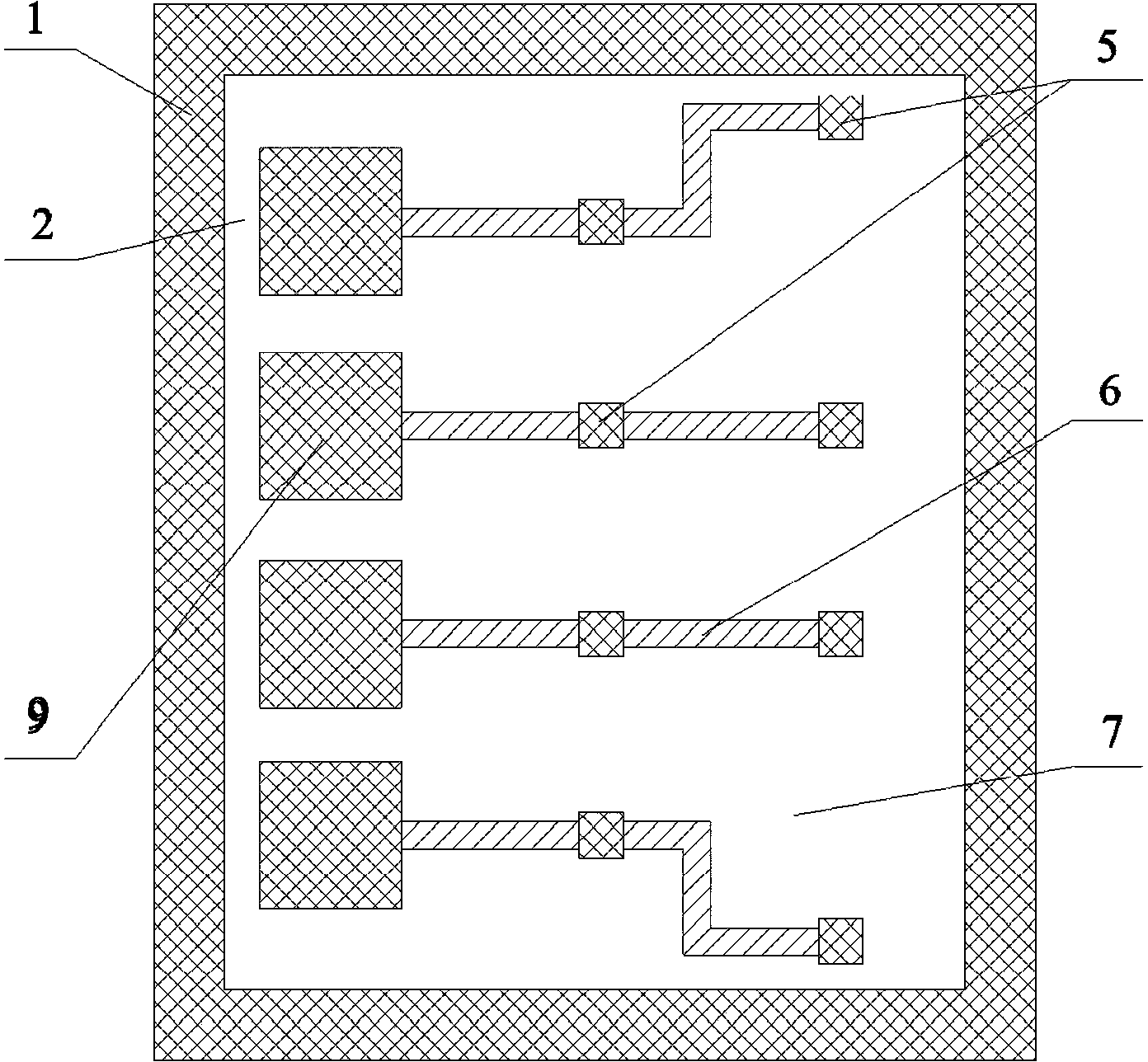
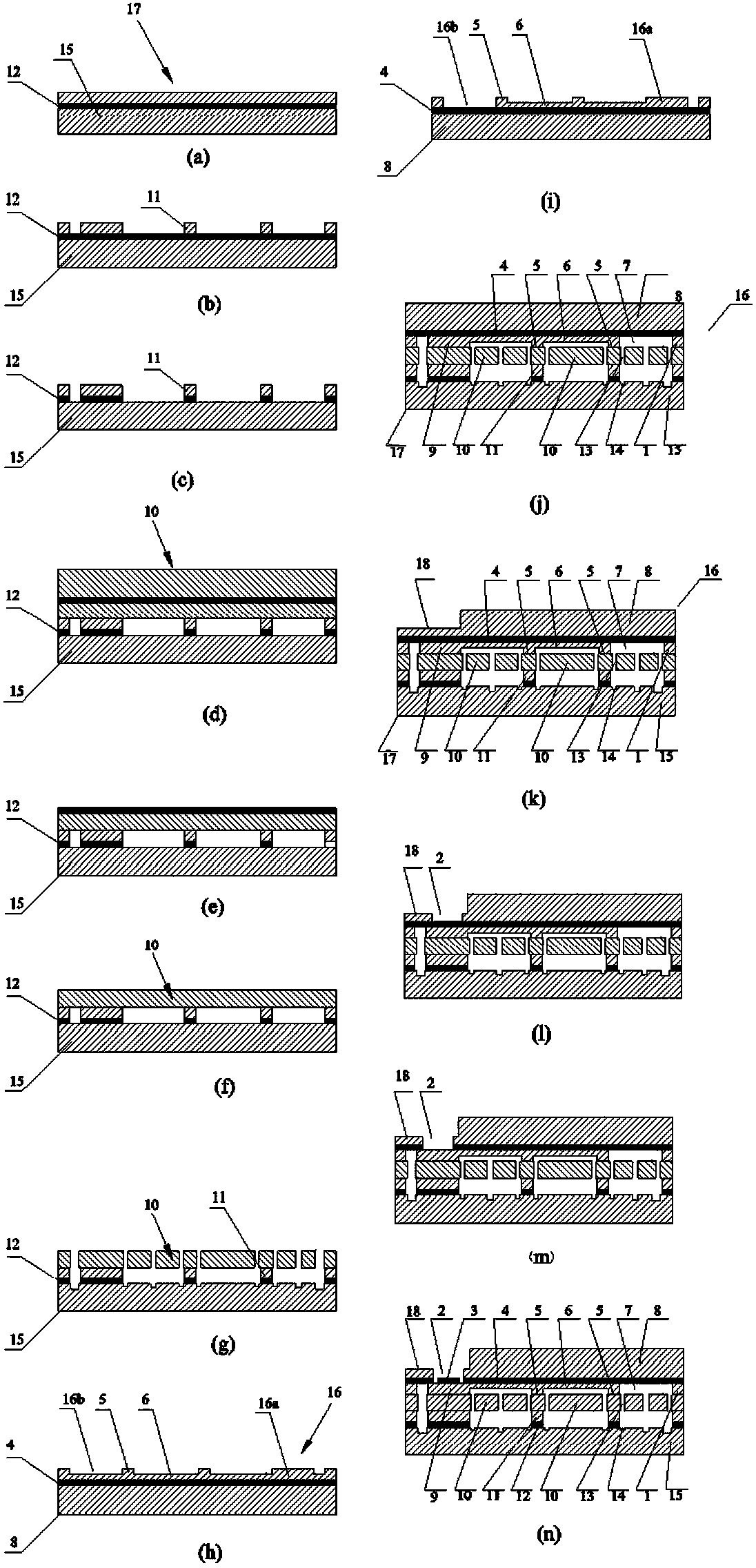
[0027] Such as figure 1 , figure 2 As shown, the MEMS device is composed of a substrate SOI silicon wafer 17 , a structural layer 10 formed of silicon on top of the SOI silicon wafer, and a cap layer SOI silicon wafer 16 . The substrate SOI silicon wafer 17 includes a substrate layer 15 , a buried oxide layer 12 and a top silicon layer 11 , and the cap SOI silicon wafer 16 includes a substrate layer 8 , a buried oxide layer 4 and a top silicon layer 6 .

[0028] The substrate SOI silicon wafer 17 includes an anchor point 11, which acts as a movable structure support, and the buried oxide layer 12 at the bottom of the anchor point 11 acts as an electrical isolation.

[0029] The device structure layer 10 is directly bonded to the substrate SOI silicon wafer 17. During the structure etching release process, etching ions in the etche...


PUM


Abstract

The invention relates to an all-silicon MEMS (Micro Electro-Mechanical Systems) device. The all-silicon MEMS device consists of a liner SOI silicon chip (17), a structural layer silicon chip (10) and a nut cap SOI silicon chip (16) which are subjected to direct silicon-silicon bonding, and is characterized in that a top silicon (6) of the structural layer silicon chip (10) and the nut cap SOI silicon chip are low-resistance silicon; the top silicon (6) of the nut cap SOI silicon chip is made into an electric interconnection wire and subjected to direct silicon-silicon bonding with the structural layer silicon through a bonding face (5); an electrical signal of the structural layer is led to a silicon electrode (9) in the nut cap SOI silicon chip through the electric interconnection wire and is electrically connected with a pressure welding point (3) on the silicon electrode (9); the silicon electrode (9) is subjected to direct silicon-silicon bonding with the structural layer silicon. The all-silicon MEMS device has the advantages that as the nut cap layer bulk silicon wires are adopted, the structural layer is prevented from pickling splash damage; as twice direct silicon-silicon bonding is adopted, residual stress is eliminated; the direct silicon-silicon bonding is good in airtightness; a getter does not need to be additionally added during vacuum packaging, so that the cost is effectively reduced.

Description

technical field [0001] The invention belongs to the field of micro-electromechanical technology, and in particular relates to a structure of an all-silicon MEMS device through a silicon lead of a cap body and a manufacturing method thereof. Background technique [0002] Micro Electro-Mechanical Systems (MEMS) is a new discipline developed on the basis of semiconductor integrated circuits. MEMS has attracted widespread attention due to its advantages of miniaturization, low power consumption, and mass production. It is widely used in automotive electronics, consumer electronics, biomedicine, aerospace, information technology and other fields. In recent years, the MEMS market has developed rapidly and has become a new economic growth point. [0003] MEMS processing technology is developed on the basis of semiconductor integrated circuits, and has formed processing methods represented by bulk silicon technology and surface sacrificial layer technology. Compared with semicondu...

Claims


Application Information

Patent Timeline
IPC IPC(8): B81B7/02B81C1/00B81C3/00
Inventor 何凯旋郭群英黄斌王鹏陈博陈璞王文婧刘磊
Owner EAST CHINA INST OF OPTOELECTRONICS INTEGRATEDDEVICE
Why Eureka
Try Eureka