Fully silicided gate electrodes and method of making the same

a gate electrode and fully silicide technology, applied in the field of semiconductor device manufacturing, can solve the problems of low current, degraded performance, effective thickness of the gate dielectric, etc., and achieve the effects of reducing or eliminating the depletion of gate electrodes, increasing the current drive of transistors, and reducing the doping density of substrates

Inactive Publication Date: 2007-11-20
GLOBALFOUNDRIES INC
View PDF5 Cites 18 Cited by
  • Summary
  • Abstract
  • Description
  • Claims
  • Application Information

AI Technical Summary

Benefits of technology

[0010]There is a need to form fully silicided gate electrodes selectively on a semiconductor device. The present invention provides a method of forming fully silicided (FUSI) gate electrodes in selected device regions of an integrated circuit. For example, the present invention may enable FUSI gate electrodes be selectively formed on FET gate devices that require threshold voltages of a workfunction in 0.3V-0.5V range, where FUSI induced increase in threshold voltage may be accommodated by reduction in doping density of the substrate, while avoiding formation of FUSI gate electrode in other devices where FUSI is not desirable due to, for example, already low threshold voltage. In addition, the present invention forms FUSI gate electrodes during a source / drain silicidation process. The use of FUSI gate electrode may possibly reduce or eliminate the gate depletion and therefore increases the current drive of transistors.

Problems solved by technology

Occurring in the vicinity of an interface between a polysilicon gate electrode and a gate dielectric, poly-depletion may lead to less induced charges in the channel region of a FET device causing lower current and degraded performance.
Compared with using polysilicon gate electrodes, the use of metal and / or FUSI gate electrodes may reduce an effective thickness of the gate dielectric, and thus increase the capacitance associated with the gate, or gate capacitance.
On the other hand, there are situations where it may be difficult to use metal gate electrodes in certain device areas having devices with multiple threshold voltages.
The standard way to reduce threshold voltage is to decrease the channel doping of the device; however, this leads to degraded short channel control.
The net result is that metal gate electrodes with workfunctions near the mid-gap of silicon do not have a device design point for FETs with a low threshold voltage.
However, performing FUSI on a FET gate with highly doped p+ polysilicon (pFET) may not necessarily create a workfunction value that is compatible or desirable for the intended devices.
Lower magnitudes of threshold voltage may create a FET with higher current and high power consumption while higher magnitudes of threshold voltage may result in a FET with lower current and lower power consumption.
This increase in threshold is often not desirable for FET devices that require low magnitudes of threshold voltage to achieve high performance.
Nevertheless, decreasing the channel doping to a critical level may create a FET that does not function properly.
If the substrate doping is too low then the source / drain regions may form a short circuit that may no longer be controllable by the gate electrode.
This could lead to a FET that cannot be turned off and thus becomes useless.

Method used


Image

  • Fully silicided gate electrodes and method of making the same
  • Fully silicided gate electrodes and method of making the same
  • Fully silicided gate electrodes and method of making the same

Examples


Embodiment Construction

[0016]In the following detailed description, numerous specific details are set forth, such as particular structures, components, materials, dimensions, processing steps and / or techniques, in order to provide a thorough understanding of the present invention. However, it will be appreciated by a person of ordinary skill in the art that the present invention may be practiced without these specific details. In other instances, well-known structures and / or processing steps may not have been described in detail in order to avoid obscuring the description of the invention.

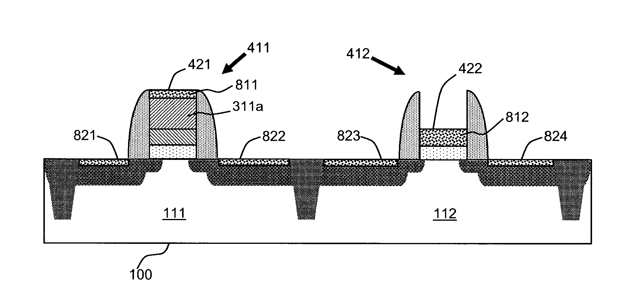
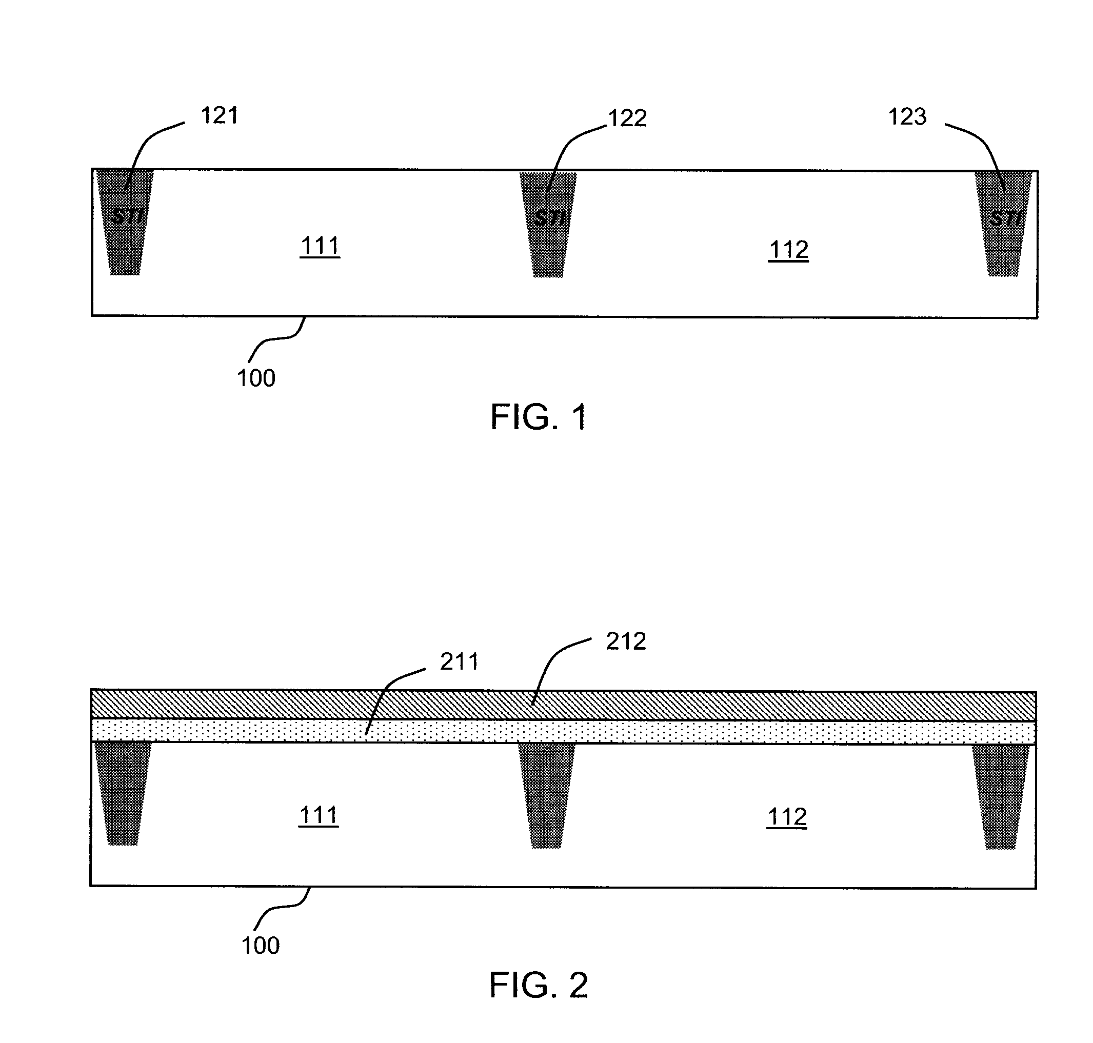
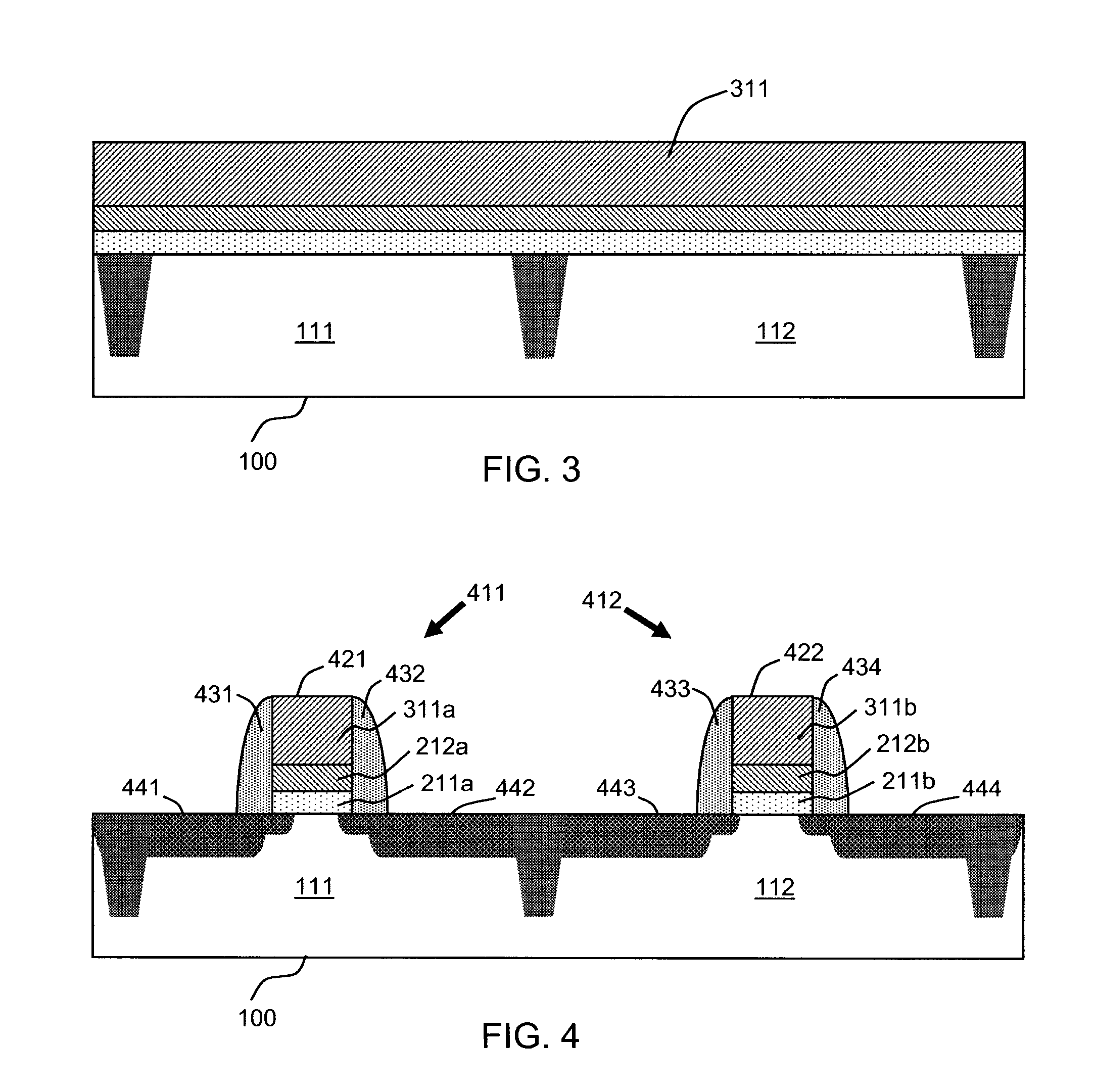
[0017]The present invention provides a method of forming fully silicided (FUSI) gate electrodes in selected device regions of an integrated circuit. For example, the present invention may enable FUSI gate electrodes be selectively formed on FET gate devices that require threshold voltages in the 0.3V-0.5V range, where FUSI induced increase in threshold voltage may be accommodated by reduction in doping density of the sub...


PUM


Abstract

The present invention relates to a method of selectively fabricating metal gate electrodes in one or more device regions by fully siliciding (FUSI) the gate electrode. The selective formation of FUSI enables metal gate electrodes to be fabricated on devices that are compatible with workfunctions that are different from conventional n+ and p+ doped poly silicon electrodes. Each device region consists of at least one Field Effect Transistor (FET) device which consists of either a polysilicon gate electrode or a fully silicided (FUSI) gate electrode. A gate electrode comprised of silicon and a Ge containing layer is used in combination with a selective removal process of the Ge containing layer. The Ge containing layer is not removed on devices with threshold voltages that are not compatible with the FUSI workfunction. Devices that are compatible with the FUSI workfunction have the Ge containing layer removed prior to the junction silicidation step. The remaining thin silicon layer of the gate electrode becomes fully silicided during the same step as the junction silicidation step.

Description

FIELD OF THE INVENTION[0001]The present invention relates to manufacture of semiconductor devices. In particular, it relates to method of making fully silicided gate electrodes for field-effect-transistors.BACKGROUND OF THE INVENTION[0002]It is well known in the art that polysilicon may be used as gate electrode in semiconductor devices such as, for example, field-effect-transistors (FETs) and in particular complementary metal-oxide-semiconductor field-effect-transistors (CMOS-FETs). On the other hand, with the continuing scaling down in dimensions of semiconductor devices, other types of gate electrodes such as, for example, metal and / or fully silicided (FUSI) gate electrodes are being used to replace the conventional polysilicon gate electrodes. Metal and / or FUSI gate electrodes may reduce and / or prevent depletion of charges, commonly known as poly-depletion, associated with polysilicon gate electrode. Occurring in the vicinity of an interface between a polysilicon gate electrode ...

Claims


Application Information

Patent Timeline
Patent Type & Authority Patents(United States)
IPC IPC(8): H01L21/28
CPCH01L21/28052H01L21/28097H01L21/324H01L21/823835H01L21/823842H01L29/665H01L29/4941H01L29/4975H01L29/517
Inventor HENSON, WILLIAM K.RIM, KERN
Owner GLOBALFOUNDRIES INC
Why Eureka
Try Eureka