Organic light-emitting diode with high color rendering

a light-emitting diode and organic technology, applied in the direction of thermoelectric device junction materials, electrical apparatus, semiconductor devices, etc., can solve the problems of high providing cost, difficult to develop an oled with excellent color rendering index and power or current efficiency at the same time, and achieve excellent color rendering index (cri) and high power or current efficiency.

Active Publication Date: 2013-10-29
NATIONAL TSING HUA UNIVERSITY
View PDF13 Cites 0 Cited by
  • Summary
  • Abstract
  • Description
  • Claims
  • Application Information

AI Technical Summary

Benefits of technology

[0008]The object of the present invention is to provide an organic light-emitting diode (OLED), which has a spacer and therefore can have excellent color rendering index (CRI) and high power or current efficiency simultaneously.
[0010]The OLED of the present invention utilizes a spacer disposed between the first light-emitting region and the second light-emitting region and therefore can obtain ideal power or current efficiency and excellent color rendering index (CRI). Compared with a conventional OLED having multi-organic layers and light-emitting layers, the OLED of the present invention has uncomplicated structure and can be easily produced with simple process due to the three layers of the light-emitting region.
[0011]According to the OLED of the present invention, the material of the spacer can be selected depending on the energy level (HOMO and LUMO) of the material. Preferably, the HOMO and LUMO energy levels of the spacer material locate between those of the first light-emitting region and the second light-emitting region, and therefore the combination of the holes and the electrons of the organic light-emitting layers can be well controlled to emit light and further to obtain excellent color rendering index (CRI). According to the present invention, the material of the spacer preferably has a hole mobility of 2×10⁻³ to 6×10⁻⁸ cm2V−1S−1. With an electric field of 3.6×10⁻⁵ Vcm−1, the electron mobility of the material of the spacer is preferably 2×10⁻³ to 6×10⁻⁸ cm2V−1S−1.

Problems solved by technology

The color rendering index (CRI) or the power or current efficiency of the OLEDs can be improved with the use of the multiple organic layers and emission layers, however it is difficult to improve the color rendering index (CRI) and the power or current efficiency simultaneously in the conventional OLEDs, whereas the multiple organic layers and emission layers may result in complex process steps that may trigger high providing cost.
Therefore, it is still difficult to develop an OLED having excellent color rendering index and power or current efficiency at the same time, which is able to replace the commonplace fluorescent lamp.

Method used


Image

  • Organic light-emitting diode with high color rendering
  • Organic light-emitting diode with high color rendering
  • Organic light-emitting diode with high color rendering

Examples


example 1

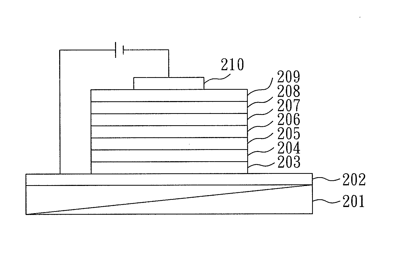
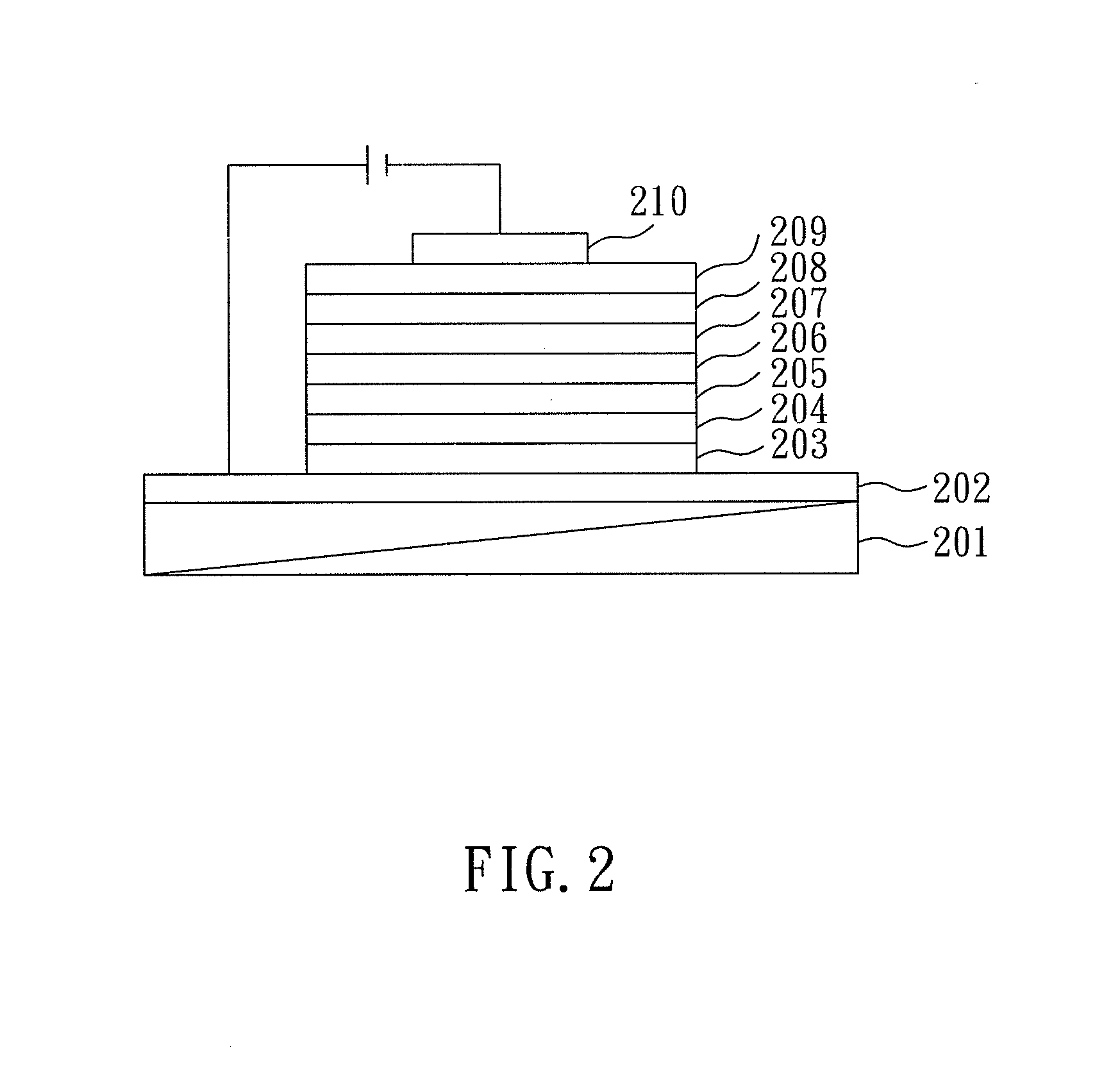
[0027]First, a substrate 201 is provided with a first electrode 202 formed thereon. Herein, the substrate 201 is a glass substrate and the first electrode 202 is an ITO anode having a thickness of 125 nm.

[0028]Then, a PEDOT:PSS polymer is coated on the first electrode 202 by spin coating to form a hole injection layer 203. After that, TAPC small molecules are vacuum evaporated to form a hole transport layer 204 on the hole injection layer 203. Herein, the hole transport layer 204 has a thickness of 10 nm.

[0029]MDP3FL as the deep blue dye and DSB as the azure dye are mixed in THF followed with vacuum drying to provide an evaporating source, which is then used to form a first light-emitting layer 205 on the hole transport layer 204, and therefore a first light-emitting region is provided. In the present example, the concentration of the DSB is 3 wt % of the MDP3FL, and the first light-emitting layer 205 has a thickness of 10 nm.

[0030]Then, a spacer 206 is formed on the first light-emi...

example 2

[0037]Except the spacer in the present example is made of TCTA, the OLED of the present example is provided by the same method as described in the Example 1.

[0038]The OLED provided by the present example is tested by a 3.5V driving voltage test and can emit white light. With brightness of 100 cd / m2, the luminescent efficiency is 12.5 Im / W; whereas with brightness of 1000 cd / m2, the luminescent efficiency is 7.5 Im / W. Meanwhile, the obtained white light from the OLED of the present example has a CIE coordinate of (0.43, 0.44) and has a CRI value of 94.

example 3

[0039]Except plural first light-emitting layer and plural second light-emitting layers are formed to provide a first light-emitting region and a second light-emitting region respectively, the OLED of the present example is provided by the same method as described in the Example 1, in which the material of each of the first light-emitting layer 205 is the same, and the material of each of the second light-emitting layer 205 is the same.

[0040]The OLED of the present invention utilizes a spacer disposed between the two light-emitting regions, in which the energy level of the spacer is adjusted to locate between the energy levels of the two light-emitting regions, and therefore can obtain ideal power or current efficiency and excellent color rendering index (CRI) with uncomplicated structure that can be provided by simple process steps. Compared with conventional OLEDs, the OLED of the present invention has uncomplicated structure and can be easily produced with simple process, and at t...


PUM


Abstract

An organic light-emitting diode with high color rendering is provided, which comprises: a substrate with a first electrode formed thereon; a first light-emitting region disposed over the first electrode, wherein the first light-emitting region comprises at least one layer of a first light-emitting layer, and the first light-emitting layer comprises at least one first dye respectively; a spacer disposed on the first light-emitting region; a second light-emitting region disposed on the organic spacer, wherein the second light-emitting region comprises at least one layer of a second light-emitting layer, and the second light-emitting layer comprises at least one second dye respectively; and a second electrode disposed over the second light-emitting region.

Description

BACKGROUND OF THE INVENTION[0001]1. Field of the Invention[0002]The present invention relates to an organic light-emitting diode and, more particularly, to an organic light-emitting diode with high color rendering.[0003]2. Description of Related Art[0004]Organic light-emitting diodes (OLEDs) are advantageous in having light weight, thinness (less than 1 mm), high brightness, wide viewing angle, no need for backlight, low energy consumption, short response time, high resolution, low heat emission, shock resistance, low producing cost, good flexibility etc, and therefore have drawn much attention to the research in the related fields.[0005]Reference with FIG. 1, wherein an organic light-emitting diode is shown, which comprises: a substrate 101, an anode 102, a hole injection layer 103, a hole transport layer 104, a light-emitting layer 105, an electron transport layer 106, an electron injection layer 108, and a cathode 108, in which the light-emitting layer 105 is disposed between the...

Claims


Application Information

Patent Timeline
Patent Type & Authority Patents(United States)
IPC IPC(8): H01L51/00
CPCH01L51/5016H01L51/5036H01L51/0085H10K85/342H10K50/11H10K2101/10H10K50/125
Inventor JOU, JWO-HUEICHOU, YI-CHIEH
Owner NATIONAL TSING HUA UNIVERSITY
Why Eureka
Try Eureka