Electrical connectivity for circuit applications

a technology for circuit applications and electrical connections, applied in the direction of electrical apparatus, semiconductor devices, semiconductor/solid-state device details, etc., can solve the problems of difficult and expensive manufacture, complicated connection of multiple transistors in parallel, and many deficiencies of conventional applications such as those discussed above, and achieves improved conductive path, easy connection, and low resisitivity

Active Publication Date: 2013-11-12
INFINEON TECH AMERICAS CORP
View PDF13 Cites 3 Cited by
  • Summary
  • Abstract
  • Description
  • Claims
  • Application Information

AI Technical Summary

Benefits of technology

[0019]Embodiments herein further include a novel integrated circuit device. The integrated circuit device can comprise a first array of switch circuits and a second array of switch circuits. The first array of switch circuits can be disposed on a semiconductor chip substrate. Each switch circuit in the first array can include a source node and a drain node. The second array of switch circuits also can be disposed on the semiconductor chip substrate. Each switch circuit in the second array can include a source node and a drain node. Source nodes in switch circuits of the first array can be disposed on the semiconductor chip substrate to be adjacent and in close proximity to source nodes in switch circuits of the second array. Accordingly, the source nodes in the first array and the second array can be easily connected to a common connectivity region of a conductive strip on the leadframe device.
[0020]In yet further embodiments as discussed herein, an integrated circuit device can include: a semiconductor layer, multiple interconnect layers, a first conductive layer and a second conductive layer. The semiconductor conductive layer can be fabricated to include multiple transistors. The multiple interconnect layers connect the multiple transistors in parallel with each other. The first conductive layer electrically can be electrically coupled to the multiple transistors via the multiple interconnect layers. The first conductive layer can be a material having a first resistivity. The second conductive layer can be electrically coupled to the first conductive layer. The second conductive layer can be a material having a second resistivity, the second resistivity being less than the first resistivity. Because the second conductive layer is a lower resisitivity, it can provide a better conductive path between, for example, transistors in the semiconductor layer and a conductive strip in the leadframe to which the conductive layers are electrically connected.

Problems solved by technology

Conventional applications such as those as discussed above can suffer from a number of deficiencies.
Connecting multiple transistors in parallel can be quite complex due to the number of individual transistors that must be interconnected.
As is known, the transistors in such a device as well as corresponding metal interconnect layers of the integrated circuit are very small and thus difficult and expensive to manufacture.
Even if it is possible to manufacture such devices, the complexity of the metal interconnect layers of the integrated circuit means that the device is more likely prone to failure or low manufacture yields.
Additionally, when used, the metalization layers in an integrated circuit are usually not thick enough to provide a very low impedance path.
This results in unwanted losses.

Method used


Image

  • Electrical connectivity for circuit applications
  • Electrical connectivity for circuit applications
  • Electrical connectivity for circuit applications

Examples


Embodiment Construction

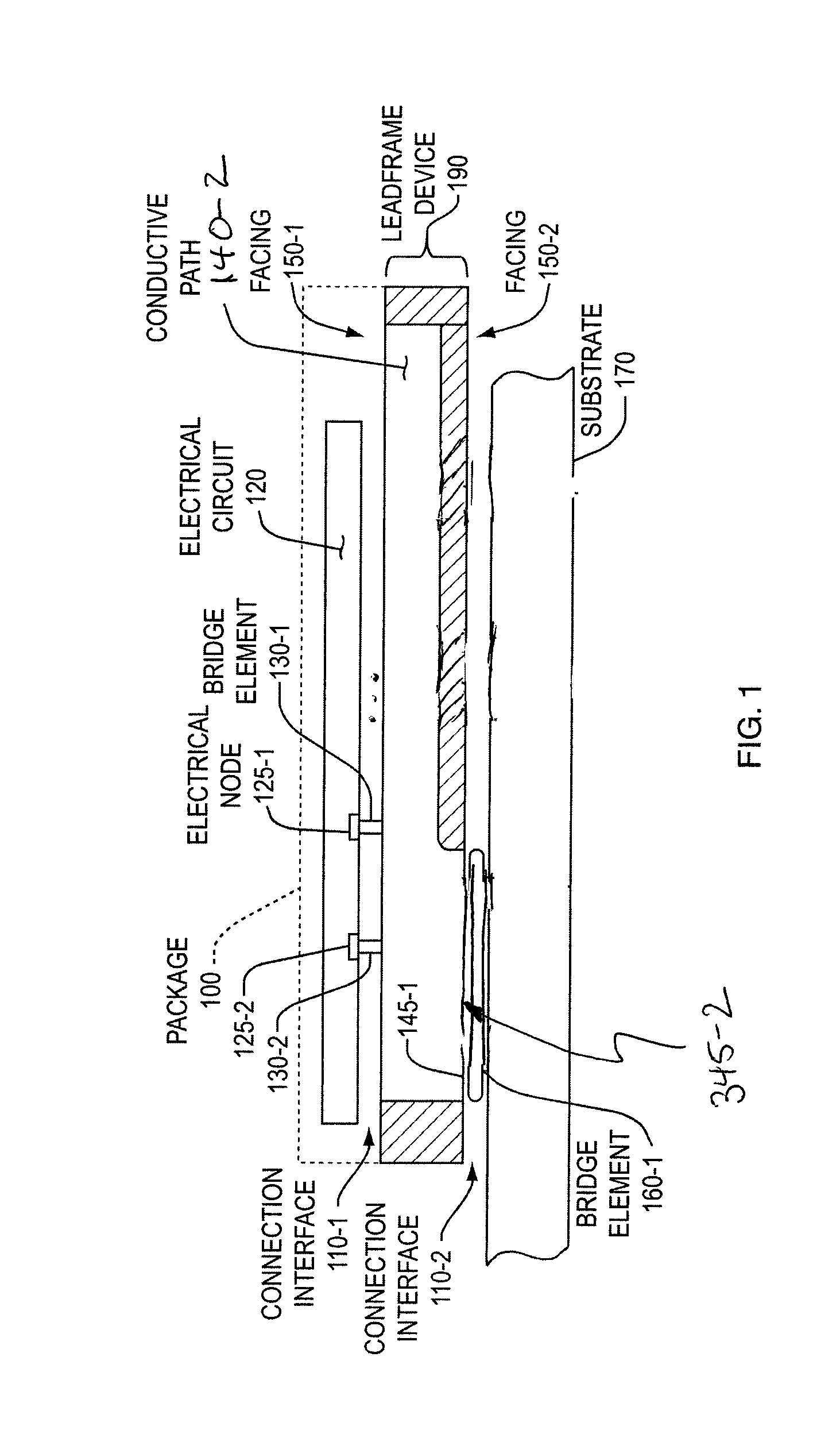
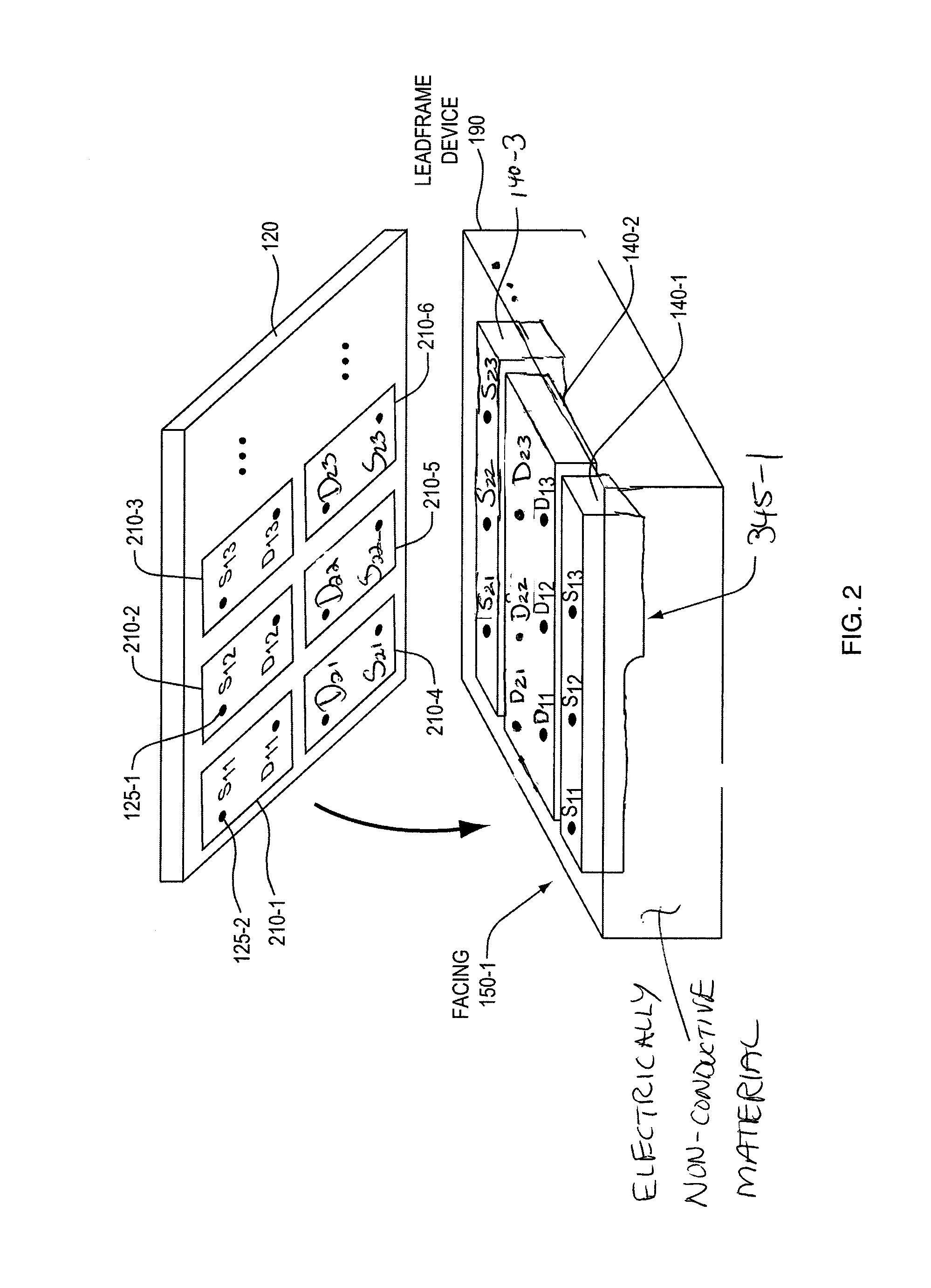
[0048]FIG. 1 is an example diagram illustrating interconnectivity of an electrical circuit 120, leadframe device 190, and substrate 170 according to embodiments herein.

[0049]As shown, one embodiment herein includes a leadframe device 190 comprising a connection interface 110-1. The connection interface 110-1 can be configured for electrically attaching or coupling electrical circuit 120 such as a semiconductor chip, integrated circuit, etc., to the leadframe device 190.

[0050]The leadframe device 190 includes one or more conductive paths including conductive path 140-2. The conductive path 140-2 (e.g., conductive strip) has a contact region on facing 150-1 of the leadframe device 190 and provides a contact region in which to make an electrical connection between electrical node 125-1 of the electrical circuit 120 and electrical node 125-2 (e.g., a source node, drain node, etc.) of the electrical circuit 120. Electrical node 125-1 can be an exposed metallic region or contact on a faci...


PUM


Abstract

According to example configurations herein, a leadframe includes a first conductive strip, a second conductive strip, and a third conductive strip disposed substantially adjacent and substantially parallel to each other. A semiconductor chip substrate includes a first array of switch circuits disposed adjacent and parallel to a second array of switch circuits. Source nodes in switch circuits of the first array are disposed substantially adjacent and substantially parallel to source nodes in switch circuits of the second array. When the semiconductor chip and the leadframe device are combined to form a circuit package, a connectivity interface between the semiconductor chip and conductive strips in the circuit package couples each of the source nodes in switch circuits of the first array and each of the multiple source nodes in switch circuits of the second array to a common conductive strip in the leadframe device.

Description

BACKGROUND[0001]Surface-mount technology (SMT) provides a way of interconnecting electronic circuit components with each other. For example, according to such technology, electronic devices are specifically packaged for mounting directly on a respective surface of a printed circuit board. Because of the advantages associated with surface mount technology such as smaller part size, surface mount technology has, to a large extent, replaced through-hole technology in which wire leads of components are fitted and soldered into holes of a printed circuit board to provide connectivity.[0002]Surface mount devices come in a variety of styles. For example, a surface mount device can have relatively small leads or no leads extending from the package at all. Because a surface mount device has relatively small leads or no leads at all, a surface mount device is usually smaller than its through-hole counterpart. The surface mount device may have short pins or leads of various styles, flat contac...

Claims


Application Information

Patent Timeline
Patent Type & Authority Patents(United States)
IPC IPC(8): H01L29/76H01L23/48
CPCH01L21/50H01L23/4824H01L23/49562H01L2224/16245H01L25/072H01L2924/1305H01L2924/00
Inventor DESBIENS, DONALD J.POLHEMUS, GARY D.CARROLL, ROBERT T.
Owner INFINEON TECH AMERICAS CORP
Why Eureka
Try Eureka