Backside dummy plugs for 3D integration

a backside dummy plug and 3d integration technology, applied in the field of semiconductor structure, can solve the problems of reducing the area available for use as active areas, reducing the overall system level performance of multiple semiconductor chips, and reducing the chip area available for use, so as to improve the vertical thermal conductivity of the semiconductor structure, enhance the inter-wafer thermal conductivity, and reduce the effect of mechanical stress on the substra

Active Publication Date: 2013-11-19
GLOBALFOUNDRIES U S INC
View PDF8 Cites 9 Cited by
  • Summary
  • Abstract
  • Description
  • Claims
  • Application Information

AI Technical Summary

Benefits of technology

[0008]The present invention provides a semiconductor structure that includes backside dummy plugs embedded in a substrate. The backside dummy plugs can be a conductive structure that enhances vertical thermal conductivity of the semiconductor structure and provides electrical decoupling of signals in through-substrate vias (TSVs) in the substrate. The backside dummy plug can include a cavity to accommodate volume changes in other components in the substrate, thereby alleviating mechanical stress in the substrate during thermal cycling and operation of the semiconductor chip. The backside dummy plug including the cavity can be composed of an insulator material or a conductive material. The cavity can be formed in a straight trench, or formed as a bottle shaped trench having a greater lateral dimension than an opening of the trench. The inventive structures can be employed to form three-dimensional structures having vertical chip integration, in which inter-wafer thermal conductivity is enhanced, cross-talk between signals through TSVs is reduced, and / or mechanical stress to the TSVs is reduced. The backside dummy plugs in a three-dimensional interconnect structure can improve thermal conductivity, signal integrity of TSVs, and / or reliability of TSVs without requiring any additional active areas.

Problems solved by technology

Such limitations are caused, for example, by inter-wafer thermal conductivity, cross-talk between signals in TSVs, and structural reliability of TSVs throughout the operational lifetime of the stacked structure.
These limitations to 3D integration can degrade the overall system level performance of a stacked structure of multiple semiconductor chips.
Addressing such challenges without sacrificing performance of semiconductor chips in the system can be difficult.
However, formation of a large number of TSVs requires use of a large chip area for TSVs, thereby reducing the chip area available for use as active areas, i.e., areas in which semiconductor devices can be built.
Increasing the number of TSVs has the effect of reducing the active areas or increasing the overall chip size, and may not be a viable solution in many instances.
However, formation of such shielding structures requires large active areas, rendering such an option practically unaffordable.
Accumulation of stress in the TSVs can cause cracking in the stacked chip structure resulting in a structural reliability problem such as dislodging of some of the TSV and subsequently vertical movement of the TSVs within a semiconductor chip.

Method used


Image

  • Backside dummy plugs for 3D integration
  • Backside dummy plugs for 3D integration
  • Backside dummy plugs for 3D integration

Examples


first embodiment

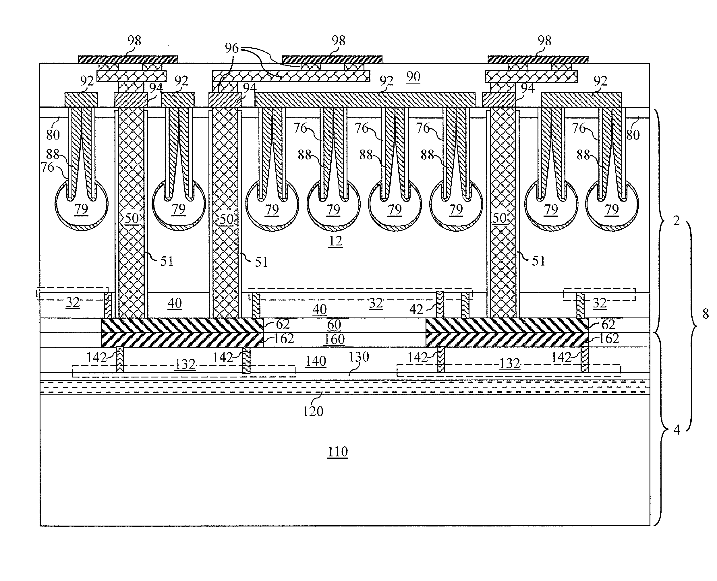
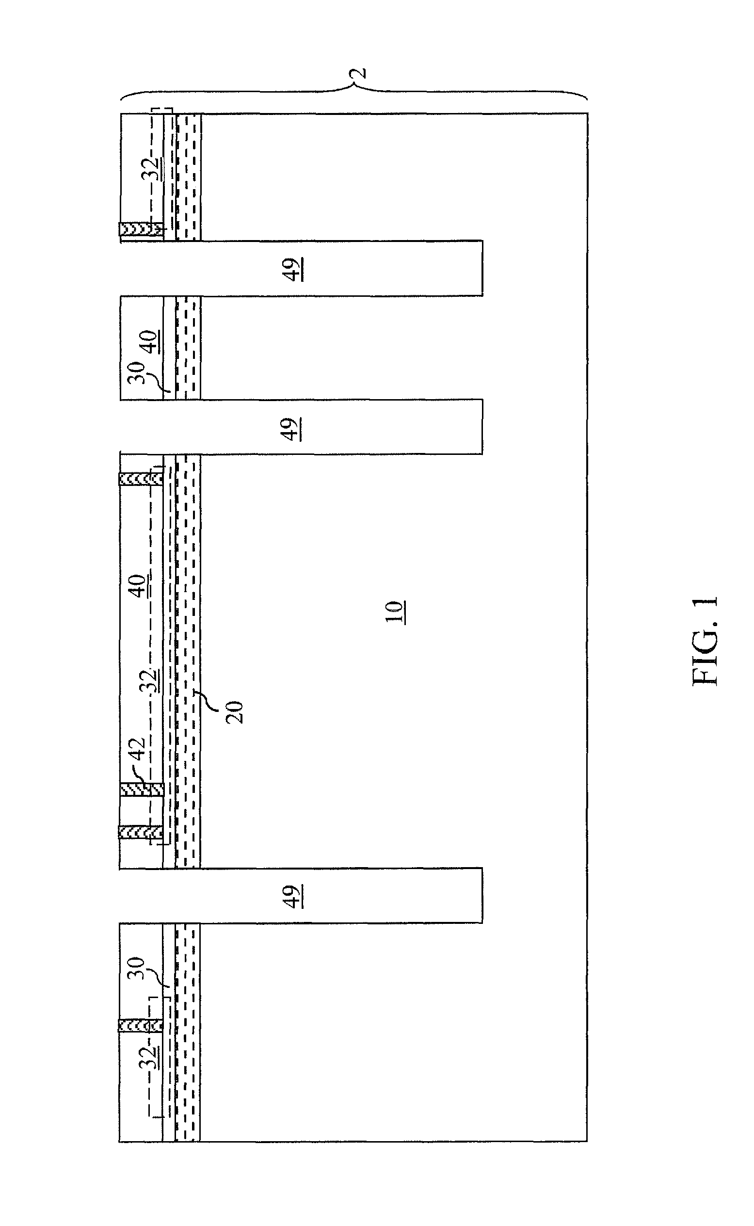
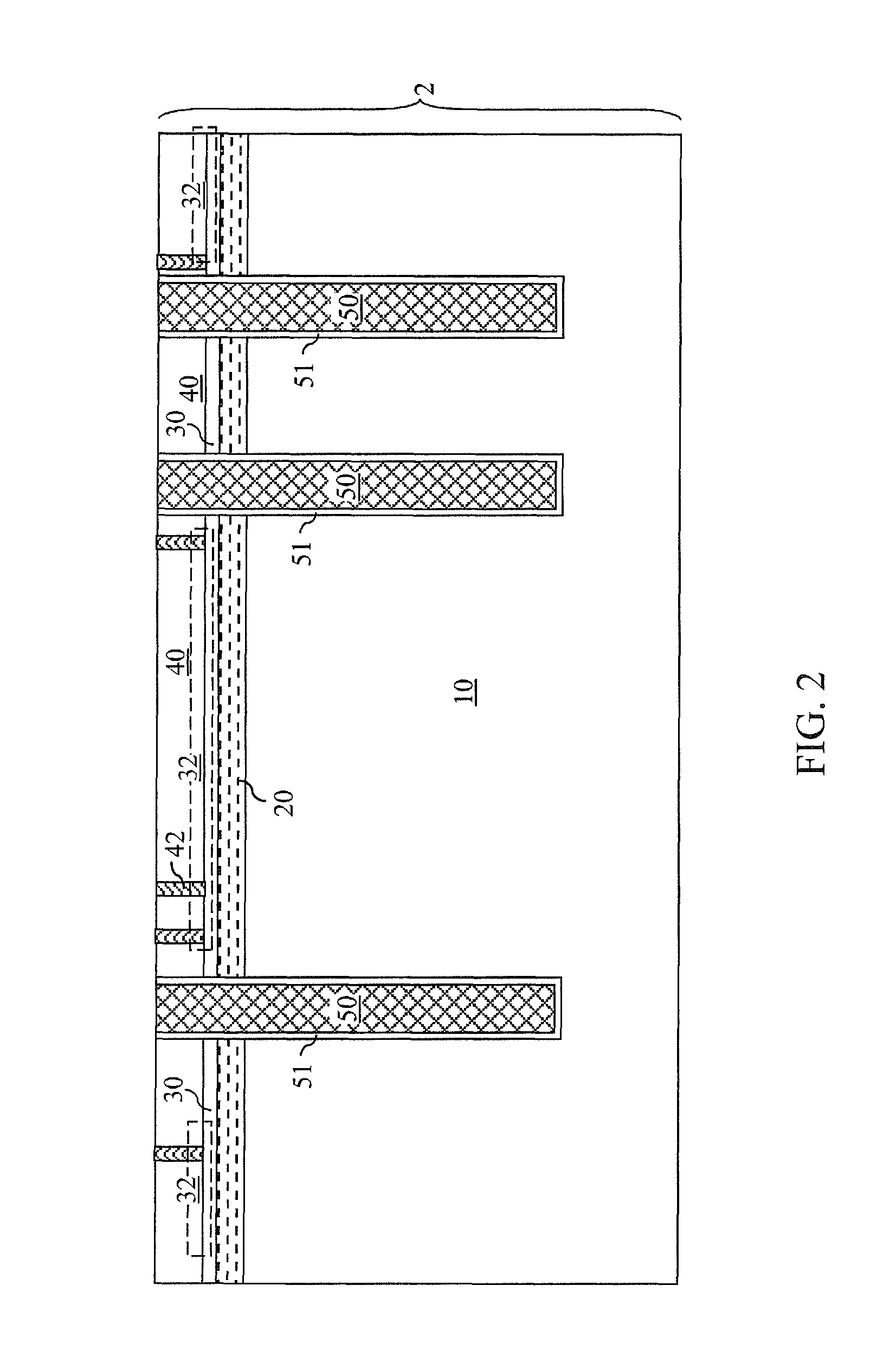
[0025]Referring to FIG. 1, a first exemplary semiconductor structure according to the present invention includes a first substrate 2. The first substrate 2 can include a semiconductor-on-insulator (SOI) substrate, a bulk semiconductor substrate, or a hybrid substrate including at least one SOI portion and at least one bulk portion. If the first substrate 2 includes an SOI substrate, the SOI substrate can contain, from bottom to top, a first handle substrate 10, a first buried insulator layer 20, and a first top semiconductor layer 30.

[0026]The first handle substrate 10 can include a semiconductor material, a dielectric material, a conductive material, or a combination thereof. Typically, the first handle substrate 20 includes a semiconductor material. The thickness of the handle substrate 10 can be from 100 microns to 1,000 microns, although lesser and greater thicknesses can also be employed. The first buried insulator layer 20 includes a dielectric material such as silicon oxide, ...

second embodiment

[0054]Referring to FIG. 11, a second exemplary semiconductor structure according to the present invention is derived from the first exemplary semiconductor structure in FIG. 7 by depositing a non-conformal dielectric material layer 74L. The thickness of the non-conformal dielectric material layer 74L is greater than one half of the lateral dimensions of the at least one trench 69. The thickness of the non-conformal dielectric material layer 74L is measured above the upper surface of the optional planarization dielectric layer 80 if the optional planarization dielectric layer 80 is present, or above the upper surface of the first handle substrate 10 if the optional planarization dielectric layer 80 is not present. Each of the at least one trench 69 in FIG. 7 is partially filled with the dielectric material of the non-conformal dielectric material layer 74L, thereby forming therein a cavity 75 surrounded by the dielectric material. Each of the at least one cavity 75 is sealed off by t...

third embodiment

[0062]Referring to FIG. 15, a third exemplary semiconductor structure according to the present invention is derived from the first exemplary semiconductor structure in FIG. 7 by depositing a non-conformal conductive material layer (not shown) instead of a non-conformal dielectric material layer 741, of FIG. 11. The thickness of the non-conformal conductive material layer is greater than one half of the lateral dimensions of the at least one trench 69. Each of the at least one trench 69 in FIG. 7 is partially filled with the conductive material of the non-conformal conductive material layer, thereby forming therein a cavity 75 surrounded by the conductive material. Each of the at least one cavity 75 is sealed off by the conductive material of the non-conformal conductive material layer. The non-conformal conductive material layer can be formed by any non-conformal deposition process that deposits a conductive material. For example, the non-conformal conductive material layer can be d...


PUM


Abstract

A semiconductor structure includes backside dummy plugs embedded in a substrate. The backside dummy plugs can be a conductive structure that enhances vertical thermal conductivity of the semiconductor structure and provides electrical decoupling of signals in through-substrate vias (TSVs) in the substrate. The backside dummy plug can include a cavity to accommodate volume changes in other components in the substrate, thereby alleviating mechanical stress in the substrate during thermal cycling and operation of the semiconductor chip. The backside dummy plug including the cavity can be composed of an insulator material or a conductive material. The inventive structures can be employed to form three-dimensional structures having vertical chip integration, in which inter-wafer thermal conductivity is enhanced, cross-talk between signals through TSVs is reduced, and / or mechanical stress to the TSVs is reduced.

Description

BACKGROUND[0001]The present invention relates to a semiconductor structure including backside dummy plugs in a substrate and methods of manufacturing the same.[0002]3D integration, or chip stacking, refers to a method of assembling two or more semiconductor chips so that the semiconductor chips that are placed in physical proximity to one another are also electrically connected among one another. 3D integration is typically performed vertically, i.e., one chip is placed above or below another chip. When two chips are brought together vertically, a set of conductive contact structures on the top surface of an underlying chip is aligned to another set of conductive contact structures on the bottom surface of an overlying chip. The conductive structures may be formed on the side of metal interconnect structures, or they may be formed on the side of a substrate on which semiconductor devices are formed.[0003]3D integration may be performed between a pair of substrates, a substrate and a...

Claims


Application Information

Patent Timeline
Patent Type & Authority Patents(United States)
IPC IPC(8): H01L23/40
CPCH01L21/768H01L21/76898H01L23/3677H01L23/481H01L23/585H01L21/7682H01L24/05H01L2924/1461H01L2225/06541H01L2924/12044H01L2224/05024H01L2224/05095H01L2224/05094H01L24/08H01L24/80H01L2224/02372H01L2224/0401H01L2224/0557H01L2224/08145H01L2224/80006H01L2924/01327H01L2924/0002H01L2224/80357H01L2224/80895H01L2224/80896H01L2224/9202H01L2924/1306H01L2924/00014H01L2924/1305H01L2924/1301H01L2924/00H01L2224/05552H01L2924/14H01L2224/80986H01L21/00H01L23/34H01L23/5226
Inventor KOESTER, STEVEN J.LIU, FEI
Owner GLOBALFOUNDRIES U S INC
Why Eureka
Try Eureka