Laminate type ceramic electronic component and manufacturing method therefor

a technology of ceramic electronic components and manufacturing methods, which is applied in the direction of fixed capacitors, variable capacitors, fixed capacitor details, etc., can solve the problems of difficult to achieve a balance between the fixing strength and film strength of the plating film described above, the gap between the plating film and the component main body, and the fixing strength. to achieve the effect of improving the fixing strength, increasing the p content rate, and increasing the hardness of the first plating layer

Active Publication Date: 2013-11-19
MURATA MFG CO LTD
View PDF22 Cites 2 Cited by
  • Summary
  • Abstract
  • Description
  • Claims
  • Application Information

AI Technical Summary

Benefits of technology

[0017]In the laminate type ceramic electronic component according to various preferred embodiments of the present invention, first, the first plating layer in the external electrode preferably is composed of the Ni—P plating film with a P content rate of about 9 weight % or more, and the fixing strength can be thus improved. More specifically, the increased P content rate increases the hardness of the plating film. Therefore, the hardness of the first plating layer can be increased. This increased hardness of the first plating layer reduces the film stress in the case of following minute concavity and convexity of the ceramic, thus increasing the anchor effect. Therefore, the joint strength of the first plating layer with the exposed ends of the internal electrodes is totally increased, and peeling is made less likely to be caused at the interface between the first plating layer and the ceramic section around the exposed ends of the internal electrodes. Thus, the reliability in moisture resistance is improved in the case of mounting.
[0018]In addition, the increased P content rate improves the corrosion resistance of the plating film. Therefore, the corrosion resistance of the first plating layer is improved, and also in this regard, the reliability in moisture resistance can be improved.
[0019]The Ni—P plating film constituting the first plating layer is preferably amorphous as described previously. The amorphous Ni—P plating film favorably follows the concavity and convexity of the ceramic as described above. Therefore, the anchor effect described above can be further increased to further increase the fixing strength, and substantially eliminate the gaps between the first plating layer and the internal electrode, and for example, the sealing property against water vapor can be made favorable to further improve the reliability in moisture resistance.
[0020]On the other hand, the first plating layer has the drawback of fragility, because of its high hardness as described above. More specifically, the first plating layer may be cracked due to a stress or a thermal shock applied during mounting and after mounting so as to decrease the reliability in moisture resistance. It is the second plating layer composed of the Ni plating film containing substantially no P that compensates for this drawback. The Ni plating film containing no P is relatively flexible. Therefore, when the first plating layer is protected with the second plating layer, the first plating layer is made less likely to break up, and the reliability in moisture resistance can be thus kept favorable by the first plating layer.
[0021]In the way described above, the external electrode can achieve a balance between the fixing strength of the plating film and the film strength (to be unlikely to be cracked) of the plating film.
[0022]According to the method for manufacturing a laminate type ceramic electronic component according to a preferred embodiment of the present invention, the first plating layer is preferably formed by electroless plating, and a plating film with a desired P content can be thus formed stably. In addition, the second plating layer is preferably formed by electrolytic plating, thus allowing the second plating layer to be formed efficiently.

Problems solved by technology

However, the plating film formed directly by plating onto a surface of the component main body has a problem with the fixing strength between the plating film and the component main body, because glass such as in the case of the paste electrode layer described above is not interposed between the plating film and the component main body.
Moreover, it is relatively difficult to achieve a balance between the fixing strength and film strength of the plating film described above.
In this case, when the plating film is soft, the plating film is unlikely to be cracked, while the stress described above causes the plating film to peel off to cause a gap between the plating film and the component main body.
Therefore, the ingress of moisture will be caused into the gap to degrade the insulation resistance, and thus possibly decrease the reliability of the laminate type ceramic electronic component.
On the other hand, when the plating film is made harder, the fixing strength is improved, while the plating film is made fragile so as to be cracked, and thus the reliability of the laminate type ceramic electronic component decreases.

Method used


Image

  • Laminate type ceramic electronic component and manufacturing method therefor
  • Laminate type ceramic electronic component and manufacturing method therefor
  • Laminate type ceramic electronic component and manufacturing method therefor

Examples


Embodiment Construction

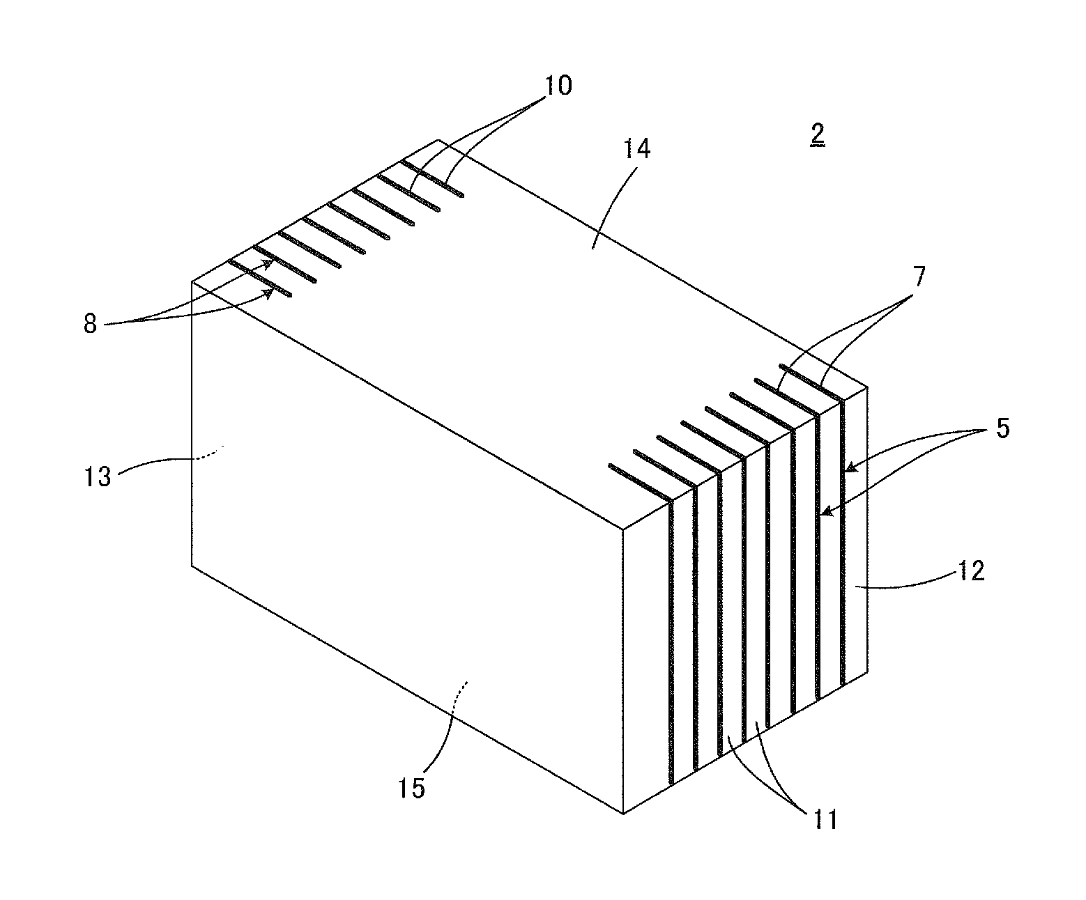
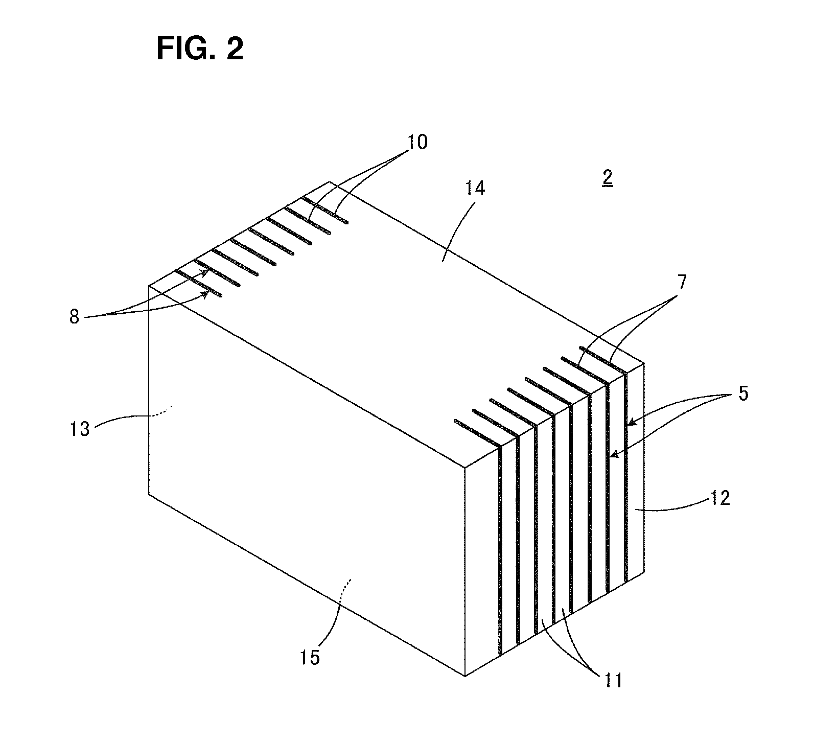
[0029]The structure of a laminated ceramic capacitor as a laminate type ceramic electronic component according to preferred embodiments of the present invention will be described in accordance with a manufacturing method therefor, with reference to FIG. 1A through FIG. 4.

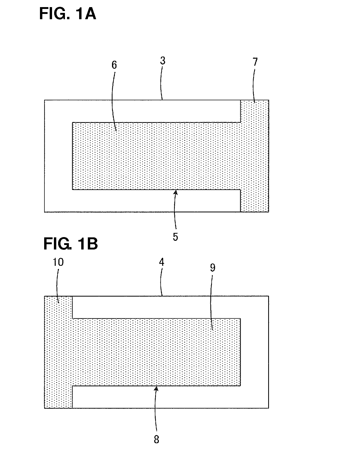
[0030]In order to manufacture a laminated ceramic capacitor 1 shown in FIG. 3, a component main body 2 shown in FIG. 2 is prepared. Furthermore, in order to obtain the component main body 2 shown in FIG. 2, two types of ceramic green sheets 3 and 4 shown in FIGS. 1A and 1B are prepared, respectively.

[0031]A first internal electrode 5 is disposed on the ceramic green sheet 3 shown in FIG. 1A. The first internal electrode 5 includes a capacitance forming section 6 constituting a main portion thereof and an extraction section 7.

[0032]The extraction section 7 extends so as to reach one short side of the ceramic green sheet 3 and to reach portions for each of two long sides adjacent to the short side, thereby constitutin...


PUM

PropertyMeasurementUnit
temperatureaaaaaaaaaa
thicknessaaaaaaaaaa

Abstract

In a laminate type ceramic electronic component, when an external electrode for a laminated ceramic capacitor is formed directly by plating onto a surface of a component main body, the film that is directly plated may have a low fixing strength with respect to the component main body. As the external electrode, a first plating layer composed of a Ni—P plating film with a P content rate of about 9 weight % or more is first formed such that a plating deposition deposited with the exposed ends of respective internal electrodes as starting points is grown on at least an end surface of a component main body. Then, a second plating layer composed of a Ni plating film containing substantially no P is formed on the first plating layer. Preferably, the first plating layer is formed by electroless plating, whereas the second plating layer is formed by electrolytic plating.

Description

BACKGROUND OF THE INVENTION[0001]1. Field of the Invention[0002]The present invention relates to a laminate type ceramic electronic component and a method for manufacturing the laminate type ceramic electronic component, and more particularly, relates to a laminate type ceramic electronic component with an external electrode including a plating film formed directly by plating so as to be electrically connected to a plurality of internal electrodes, and a method for manufacturing the laminate type ceramic electronic component.[0003]2. Description of the Related Art[0004]As shown in FIG. 5, a laminate type ceramic electronic component 101 typified by a laminated ceramic capacitor generally includes a component main body 105 having a stacked structure, which includes a plurality of stacked ceramic layers 102 composed of, for example, a dielectric ceramic, and a plurality of layered internal electrodes 103 and 104 formed along the interfaces between the ceramic layers 102. The respectiv...

Claims


Application Information

Patent Timeline
Patent Type & Authority Patents(United States)
IPC IPC(8): H01G4/30
CPCH01G4/005H01G4/30H01G4/12Y10T29/43
Inventor OGAWA, MAKOTOMOTOKI, AKIHIROSASABAYASHI, TAKEHISAKAYATANI, TAKAYUKI
Owner MURATA MFG CO LTD
Why Eureka
Try Eureka