Method of adjustment on manufacturing of a circuit having a resonant element

a manufacturing method and technology of a resonant element, applied in the field of adjustment on manufacturing of a circuit having a resonant element, can solve the problems of acoustic waves, mechanical disturbance, and difficulty in obtaining the desired oscillation frequency accuracy in manufacturing, and achieve the effect of minimizing or suppressing the calibration switched capacitor network and minimizing the inaccuracy of the oscillation frequency

Active Publication Date: 2013-11-19
STMICROELECTRONICS SRL
View PDF8 Cites 4 Cited by
  • Summary
  • Abstract
  • Description
  • Claims
  • Application Information

AI Technical Summary

Benefits of technology

[0023]One embodiment of the present disclosure provides a method for forming oscillators with BAW resonators that minimizes the inaccuracy of the oscillation frequency, and minimizing or suppressing the calibration switched capacitor network.

Problems solved by technology

When an electric field is created in the piezoelectric layer by application of a potential difference between electrodes, this results in a mechanical disturbance in the form of acoustic waves.
In practice, it is difficult in manufacturing to obtain an oscillation frequency with the desired accuracy.
A first source of inaccuracy is due to the BAW resonator manufacturing dispersions.
Indeed, methods of deposition of the different layers of a BAW resonator do not enable obtaining a resonance frequency with the desired accuracy.
Despite this adjustment, the accuracy of the BAW resonators is not ideal.
A second source of inaccuracy results from manufacturing discrepancies in the elements of circuit 23.
A disadvantage of this calibration mode is that, to be able to compensate for the above-mentioned significant inaccuracy of the oscillation frequency, a large network of switched capacitors must be provided.

Method used


Image

  • Method of adjustment on manufacturing of a circuit having a resonant element
  • Method of adjustment on manufacturing of a circuit having a resonant element
  • Method of adjustment on manufacturing of a circuit having a resonant element

Examples


Embodiment Construction

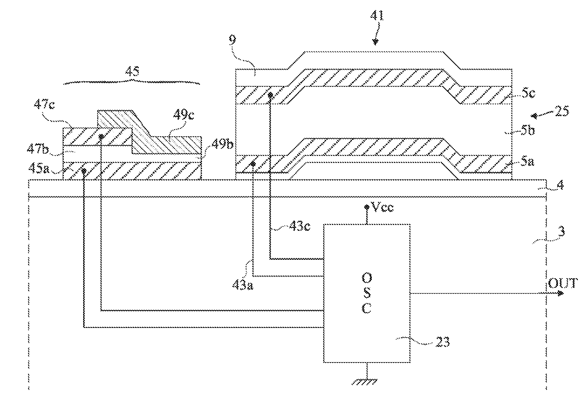
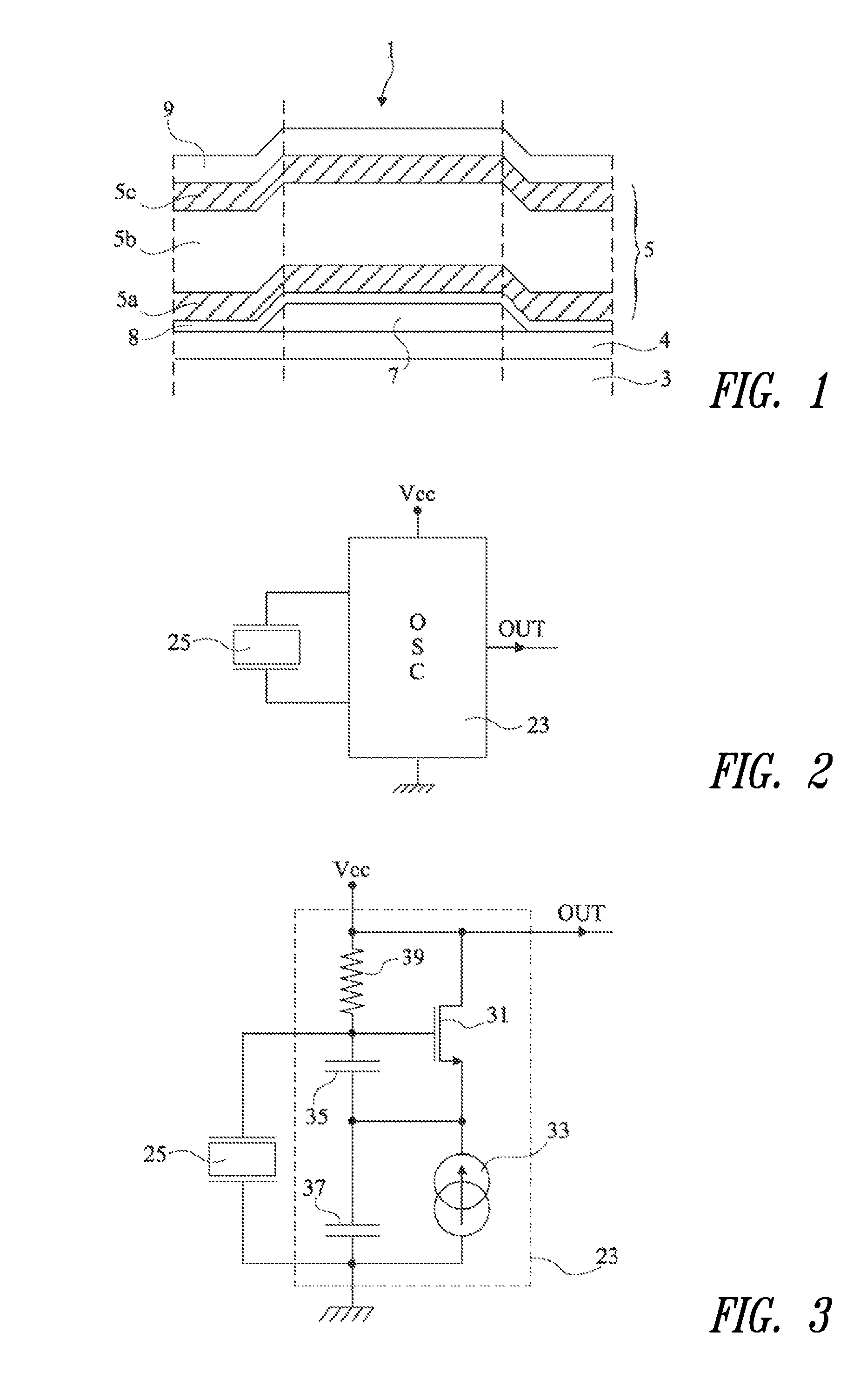
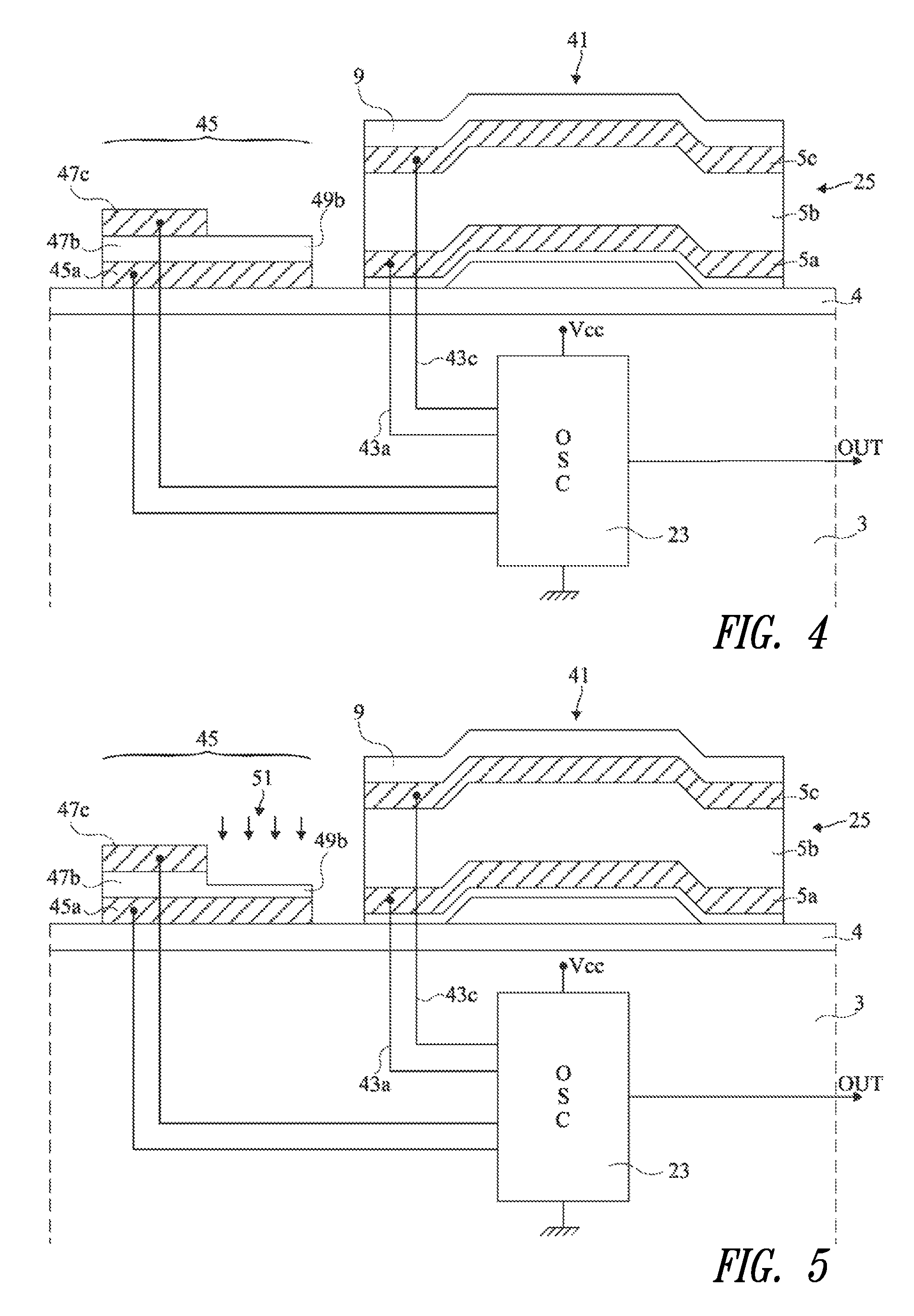
[0043]For clarity, the same elements have been designated with the same reference numerals in the different drawings and, further, as usual in the representation of integrated circuits, the various drawings are not to scale.

[0044]FIGS. 4 to 6 are cross-section views schematically illustrating steps of an example of a method of adjustment on manufacturing of an oscillator with a BAW resonator.

[0045]FIGS. 4 to 6 schematically show an embodiment of a monolithic oscillator with a BAW resonator 41 formed inside and on top of a semiconductor substrate 3 coated with an insulator 4. It should be noted that the presence of insulator 4 is optional. Although each of these drawings shows a single oscillator, in practice, many oscillators are formed simultaneously inside and on top of a same semiconductor wafer.

[0046]Various elements of a circuit 23, connected between a terminal of high voltage VCC and a terminal of low voltage, for example, the ground, are formed inside and on top of substrate ...


PUM

PropertyMeasurementUnit
surface areaaaaaaaaaaa
thicknessaaaaaaaaaa
frequencyaaaaaaaaaa

Abstract

A method of adjustment in the manufacture of a capacitance of a capacitor supported by a substrate, the method including the steps of: a) forming a first electrode parallel to the surface of the substrate and covering it with a dielectric layer; b) forming, on a first portion of the dielectric layer, a second electrode; c) measuring the capacitance between the first electrode and the second electrode, and deducing therefrom the capacitance to be added to obtain the desired capacitance; d) thinning down a second portion of the dielectric layer, which is not covered by the second electrode, so that the thickness of this second portion is adapted to the forming of the deduced capacitance; and e) forming a third electrode on the thinned-down portion and connecting it to the second electrode.

Description

BACKGROUND[0001]1. Technical Field[0002]The present disclosure relates to a method of adjustment during the manufacture of a capacitor laid on a substrate and, by way of example, the present disclosure relates to a method of manufacturing that provides for adjusting the frequency of a circuit having a resonant element, for example, a monolithic oscillator using bulk acoustic wave (BAW) resonators.[0003]2. Description of the Related Art[0004]Oscillators are mainly used in electronic devices to provide clock signals at reference frequencies. Currently, an oscillator includes oscillating circuit elements and a quartz resonator that enables accurately setting the oscillation frequency. An alternative to quartz oscillators is the use of oscillators based on[0005]BAW resonators. The use of BAW resonators enables implementing higher oscillation frequencies, for example, approximately ranging from a few hundreds of MHz to a few tens of GHz. Lower clock frequencies may also be generated by u...

Claims


Application Information

Patent Timeline
Patent Type & Authority Patents(United States)
IPC IPC(8): H01G4/005H01G4/06
CPCH01G4/228H01G4/255H01G13/06H01L22/14H01L22/20H03H3/04H01L28/60Y10T29/43H01L2924/0002Y10T29/49004H01L2924/00
Inventor BAR, PIERREJOBLOT, SYLVAINPETIT, DAVID
Owner STMICROELECTRONICS SRL
Why Eureka
Try Eureka