Semiconductor device and method of manufacturing the same

a semiconductor and device technology, applied in semiconductor devices, semiconductor/solid-state device details, electrical apparatus, etc., can solve the problems of reducing so as to reduce the reliability of connection of bumps and reduce the viscosity of polymers. , the effect of low heat resistan

Inactive Publication Date: 2013-12-31
HITACHI LTD
View PDF5 Cites 6 Cited by
  • Summary
  • Abstract
  • Description
  • Claims
  • Application Information

AI Technical Summary

Benefits of technology

[0012]However, in the case of the above-described conventional example 1, when the bump is formed by using the CMP method, there is a problem that planarity of a surface of the silicon substrate is decreased due to the cutting off of a part of the bump, the local cutting off of the benzocyclobutene (polymer film) between the adjacent bumps, or others upon the CMP, and therefore, the connection reliability of the bump is decreased when the silicon substrates are stuck to each other.
[0028]According to the present invention, a connection reliability of a bump electrode for electrically connecting substrates to each other can be improved.

Problems solved by technology

However, in the case of the above-described conventional example 1, when the bump is formed by using the CMP method, there is a problem that planarity of a surface of the silicon substrate is decreased due to the cutting off of a part of the bump, the local cutting off of the benzocyclobutene (polymer film) between the adjacent bumps, or others upon the CMP, and therefore, the connection reliability of the bump is decreased when the silicon substrates are stuck to each other.
If the number of bumps per silicon substrate is numerously increased in order to maintain the planarity of the surface of the silicon substrate, the maximum load (about 100 kN) of a commercialized bonding machine is not sufficiently enough to obtain the bonding between the copper bumps, and therefore, there is a problem of the decrease in the connection reliability of the bump electrode.

Method used


Image

  • Semiconductor device and method of manufacturing the same
  • Semiconductor device and method of manufacturing the same
  • Semiconductor device and method of manufacturing the same

Examples


first embodiment

[0051](First Embodiment)

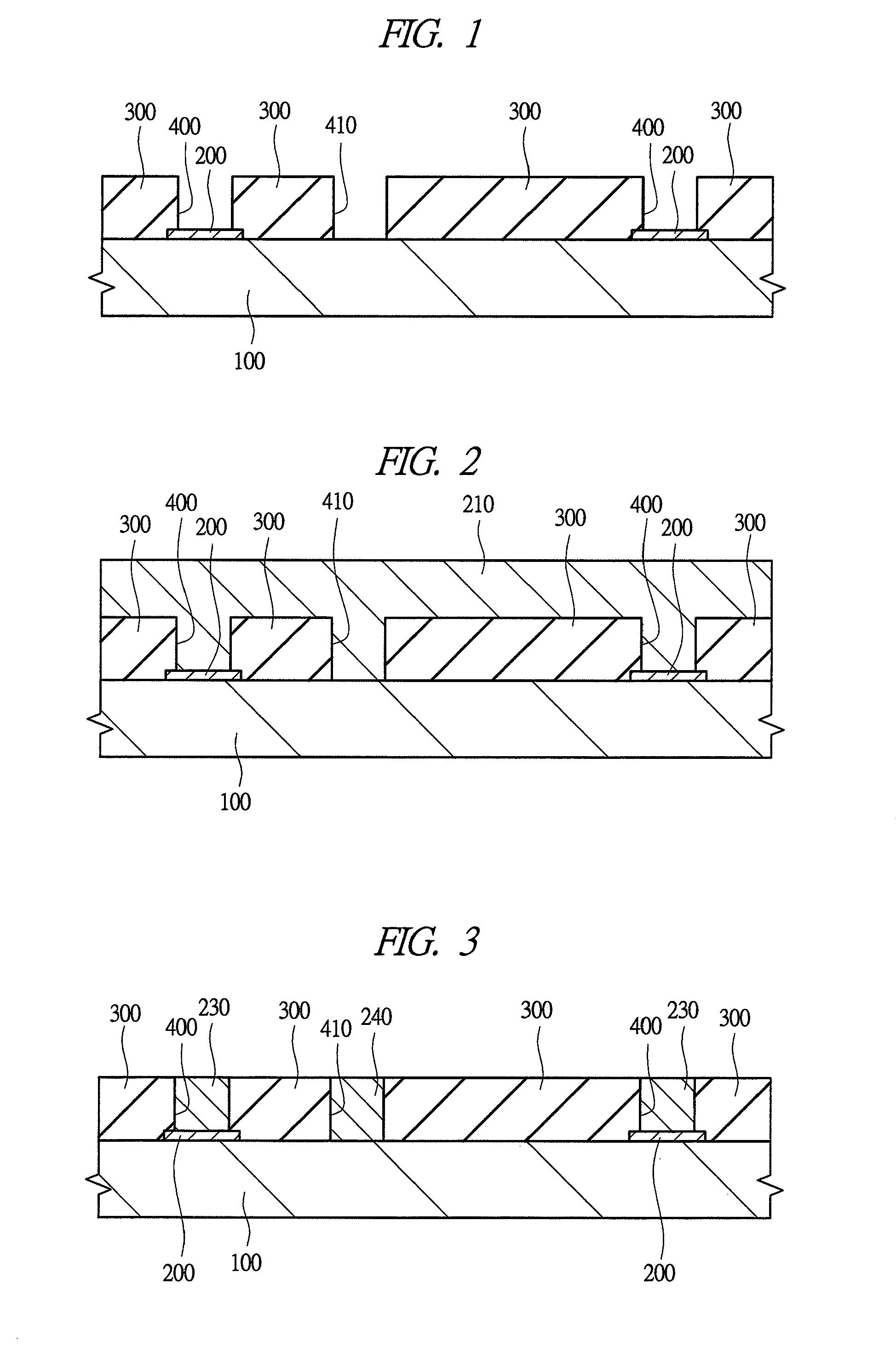
[0052]A semiconductor device according the present embodiment is a layered-type semiconductor device obtained by bonding two silicon wafers on whose main surfaces a plurality of bump electrodes and a polymer film for surrounding their peripheries are formed, and electrically connecting integrated circuits to each other formed on the respective silicon wafers via a bump electrode.

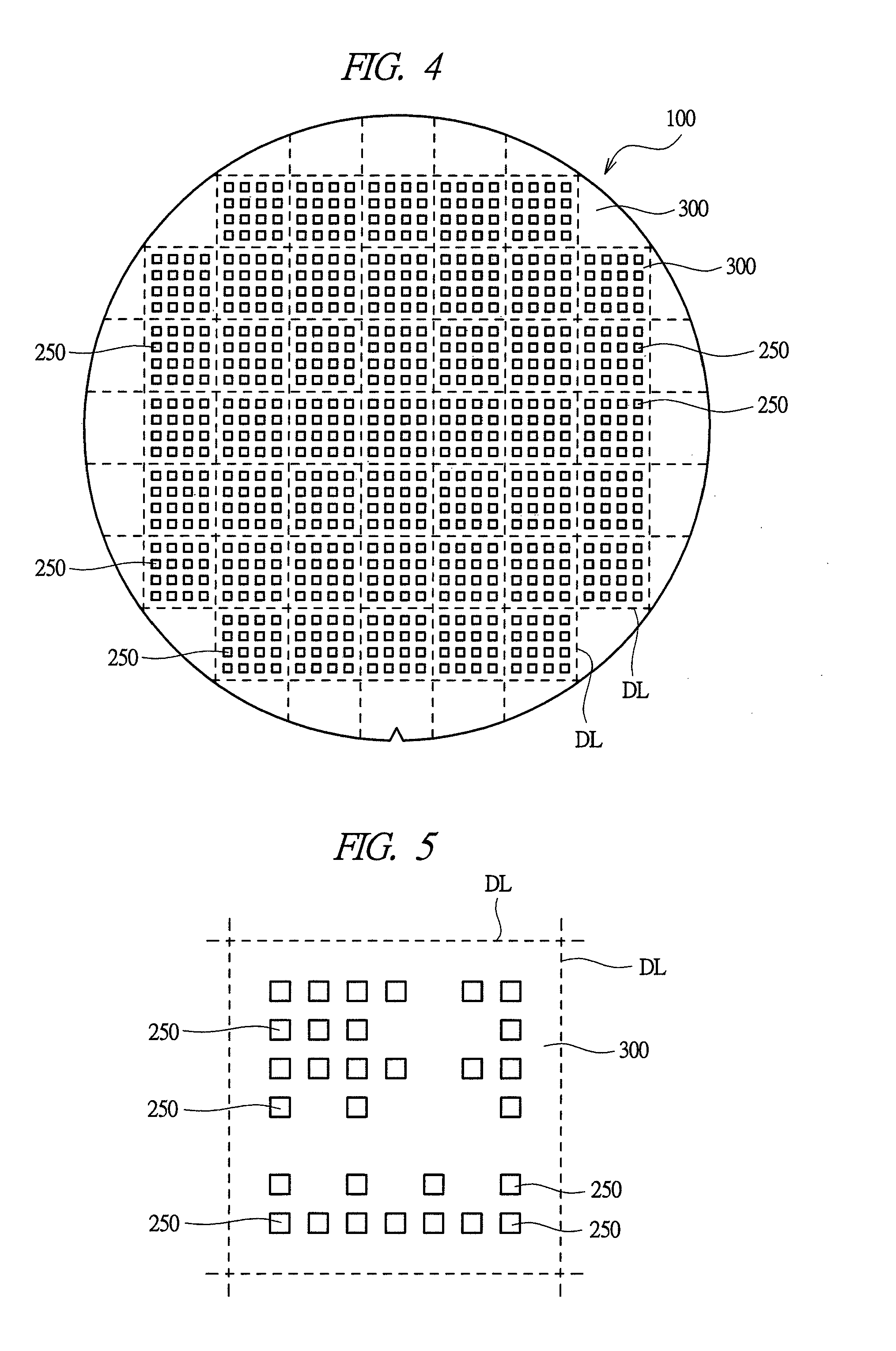
[0053]Hereinafter, with reference to FIGS. 1 to 9, a method of manufacturing the semiconductor device of the present embodiment will be explained in an order of steps. FIGS. 1 to 3, 7 and 8 are cross-sectional views of principal parts each explaining a manufacturing step for a layered semiconductor according to the first embodiment of the present invention, FIGS. 4 to 6 are planar layouts illustrating arrangement of the bump of the layered semiconductor during the manufacturing step, and FIG. 9 is a planar layout illustrating a modification example of the semiconductor device of the p...

second embodiment

[0128](Second Embodiment)

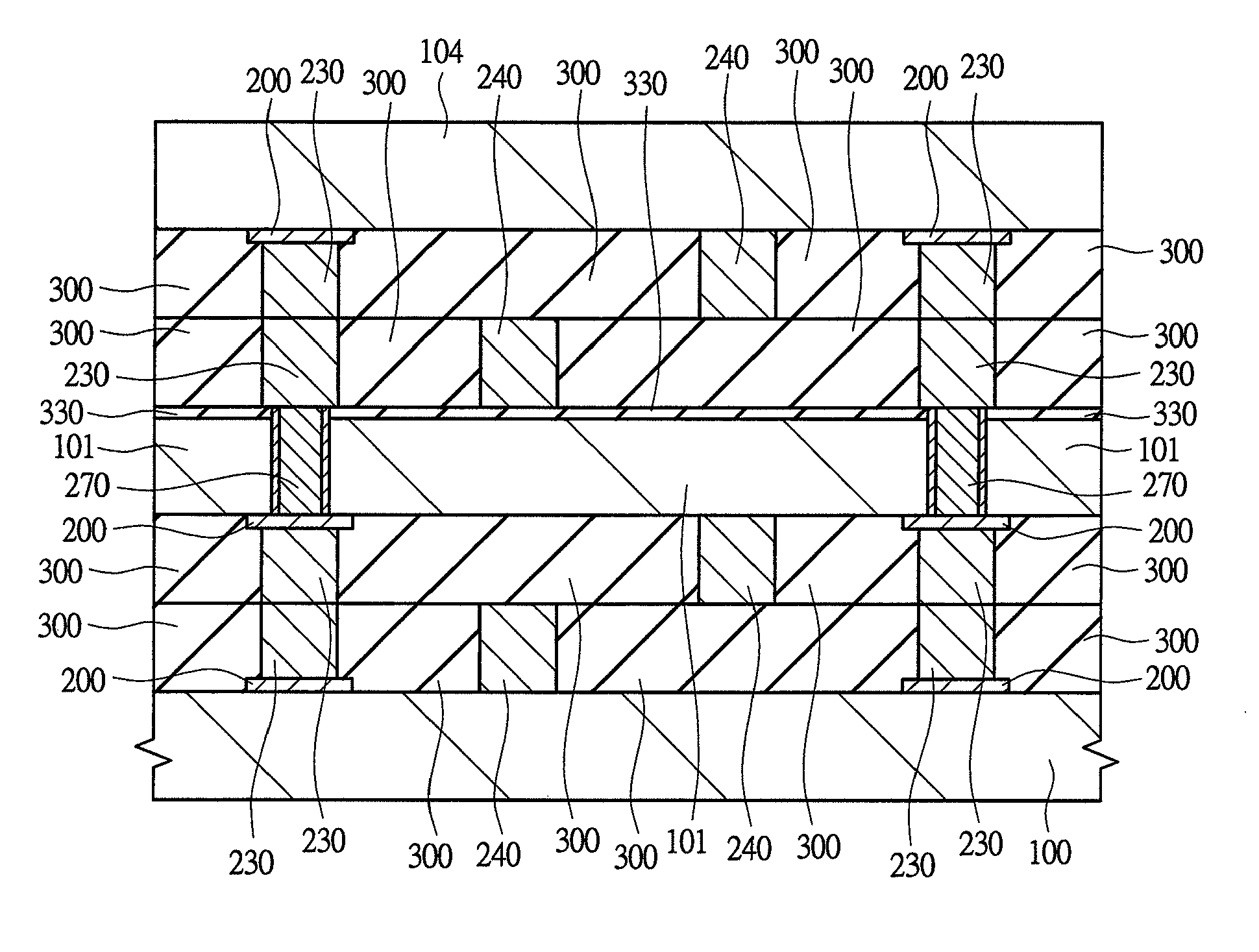
[0129]In a present embodiment, an example of a semiconductor device obtained by bonding a front surface of a silicon substrate on which a semiconductor element is formed and a rear surface on which the semiconductor element is not formed to each other will be explained with reference to FIGS. 11 to 14. Note that the explanation of a configuration with the same reference symbols and portions having the same functions as those of the configuration described above in the first embodiment will be omitted. FIGS. 11 to 14 are cross-sectional views of principal parts each explaining a manufacturing process of a layered semiconductor of the present embodiment.

[0130]First, as illustrated in FIG. 11, a rear-surface insulating film 330 formed of, for example, a silicon oxide film is formed on a rear surface of a first silicon substrate 100 on which a semiconductor element is not formed, and then, a through electrode 270 for electrical connection to a main surface of th...


PUM

PropertyMeasurementUnit
melting pointaaaaaaaaaa
temperatureaaaaaaaaaa
melting pointaaaaaaaaaa

Abstract

A bump electrode, a dummy bump, and a heat-resistant polymer film, whose upper-surface heights are uniformed, are formed on each of a first silicon substrate and a second silicon substrate, and then, the first silicon substrate and the second silicon substrate are bonded to each other so that the bump electrodes formed on the respective substrates are electrically connected to each other. At this time, the dummy bump is arranged so as to be bonded to the heat-resistant polymer film on the silicon substrate opposed thereto, so that a semiconductor device having both of good electrical connection between the bump electrodes and bump protection performance obtained by a polymer film with high heat resistance and without voids can be achieved.

Description

CROSS-REFERENCE TO RELATED APPLICATION[0001]The present application claims priority from Japanese Patent Application No. 2011-087061 filed on Apr. 11, 2011, the content of which is hereby incorporated by reference into this application.TECHNICAL FIELD OF THE INVENTION[0002]The present invention relates to a semiconductor device and a method of manufacturing the same. More particularly, the present invention relates to a technique effectively applied to a semiconductor device in which a plurality of semiconductor substrates are electrically connected to each other via a bump electrode, and a method of manufacturing the same.BACKGROUND OF THE INVENTION[0003]In recent years, as one of methods of achieving a miniaturized and high-performance semiconductor device, a mounting technique of laminating semiconductor substrates (hereinafter, referred to as silicon substrates) each made of monocrystalline silicon and electrically connecting the silicon substrates to each other by using a fine ...

Claims


Application Information

Patent Timeline
Patent Type & Authority Patents(United States)
IPC IPC(8): H01L23/52H01L23/48
CPCH01L24/81H01L2225/06513H01L25/0657H01L2224/94H01L2224/0401H01L24/83H01L2224/81193H01L2225/06517H01L2224/83203H01L2224/05009H01L2224/05624H01L2224/1145H01L24/11H01L24/14H01L2224/2919H01L2224/0345H01L2224/9211H01L2224/14181H01L2224/0362H01L2224/26125H01L24/94H01L24/32H01L24/73H01L2225/06541H01L2924/10253H01L2225/06565H01L2224/73104H01L24/16H01L2224/13025H01L24/92H01L2224/16145H01L2224/92125H01L2224/32145H01L2224/11616H01L2224/81203H01L23/481H01L2224/16225H01L2924/14H01L2224/1148H01L2924/00015H01L2224/81H01L2224/83
Inventor TAKEDA, KENICHIAOKI, MAYUHOZAWA, KAZUYUKI
Owner HITACHI LTD
Why Eureka
Try Eureka