Method and apparatus for energy harvesting using CMOS sensor

a technology of cmos sensor and energy harvesting, applied in the field of electromechanical sensors, can solve the problems of large power consumption limitation of portable/mobile systems, long operational time of devices without human intervention for energy replenishment, and undesirable human intervention, and achieve the effect of reducing the power consumed from a conventional power supply

Active Publication Date: 2014-01-14
THE HONG KONG UNIV OF SCI & TECH
View PDF4 Cites 10 Cited by
  • Summary
  • Abstract
  • Description
  • Claims
  • Application Information

AI Technical Summary

Benefits of technology

[0011]According to another embodiment, a method is provided for using an image sensor array to harvest energy from the light impinging on the sensor. The method utilizes an asynchronous readout technique, where highly illuminated pixels charge up quickly and the output signals are read out from these pixels first, due to the fact that the electrical charge reaches the predetermined threshold earlier in these pixels than in other pixels receiving lower illumination. Once the output signals are collected, these highly illuminated pixels are configured to harvest energy at earlier times than those pixels exposed to lower illumination. When a group of pixels are switch to the energy harvesting mode, the electrical charge in these pixels is used to contribute to the global power supply, thereby reducing power consumption from the main power supply. As the process continues, more and more pixels are switched to the energy harvesting mode, thereby creating an avalanche effect.

Problems solved by technology

Therefore, power consumption is a major limitation in these portable / mobile systems since the capacity of the batteries often limits their operational time.
In the case of sensor network, where the scarcest resource is energy, devices are expected to have a long operational time without human intervention for energy replenishment.
Human intervention is undesirable due to the cost of checking a large number of devices.
Low supply voltage, however, is not preferable in CMOS image sensors as it has an enormous impact on imaging performance due to limited signal swing and reduced signal-to-noise ratio (SNR).
However, the existing approach suffers several drawbacks: 1) Significant silicon area is dedicated to the photodetector used for power generation.
Poor illumination will elongate this period, thus leading to a very slow operation of the sensor.

Method used


Image

  • Method and apparatus for energy harvesting using CMOS sensor
  • Method and apparatus for energy harvesting using CMOS sensor
  • Method and apparatus for energy harvesting using CMOS sensor

Examples


Embodiment Construction

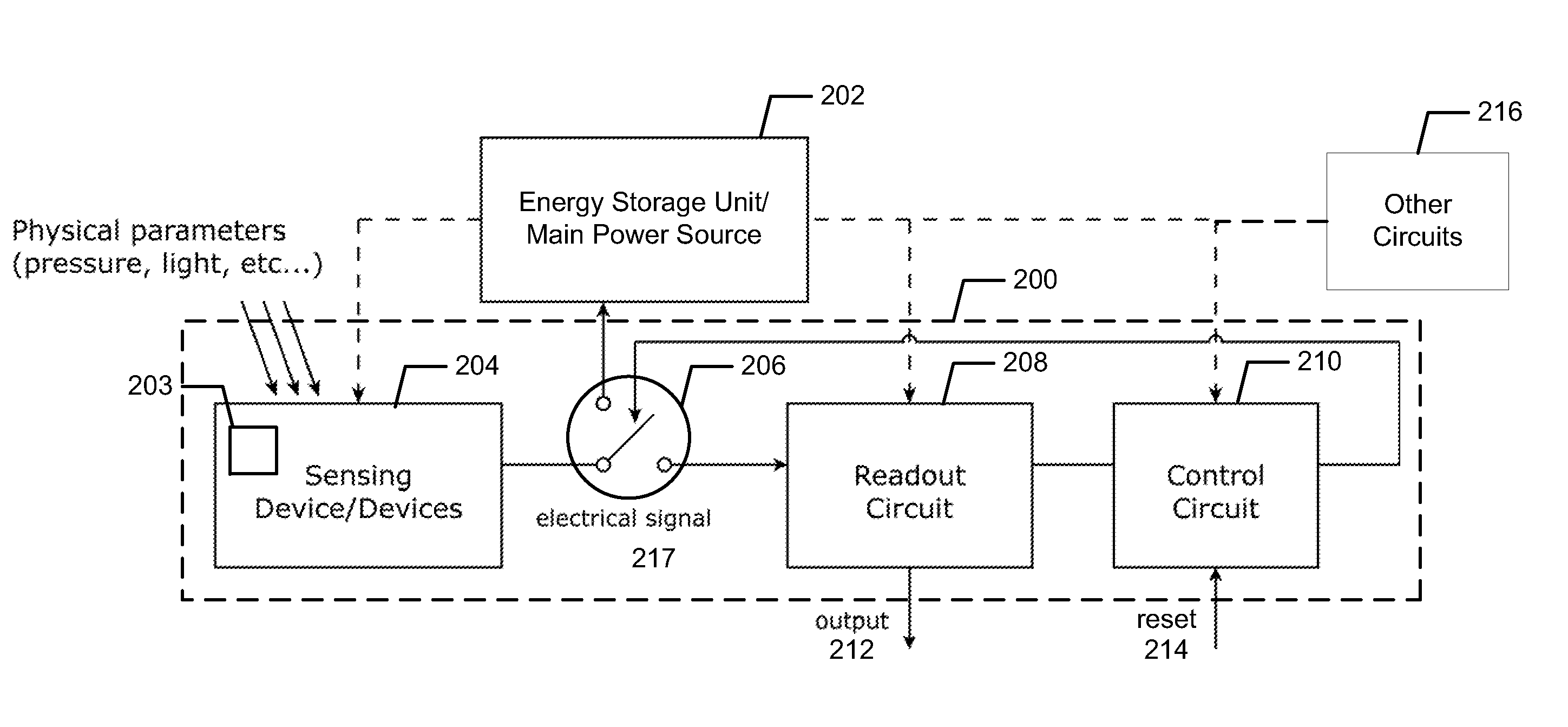
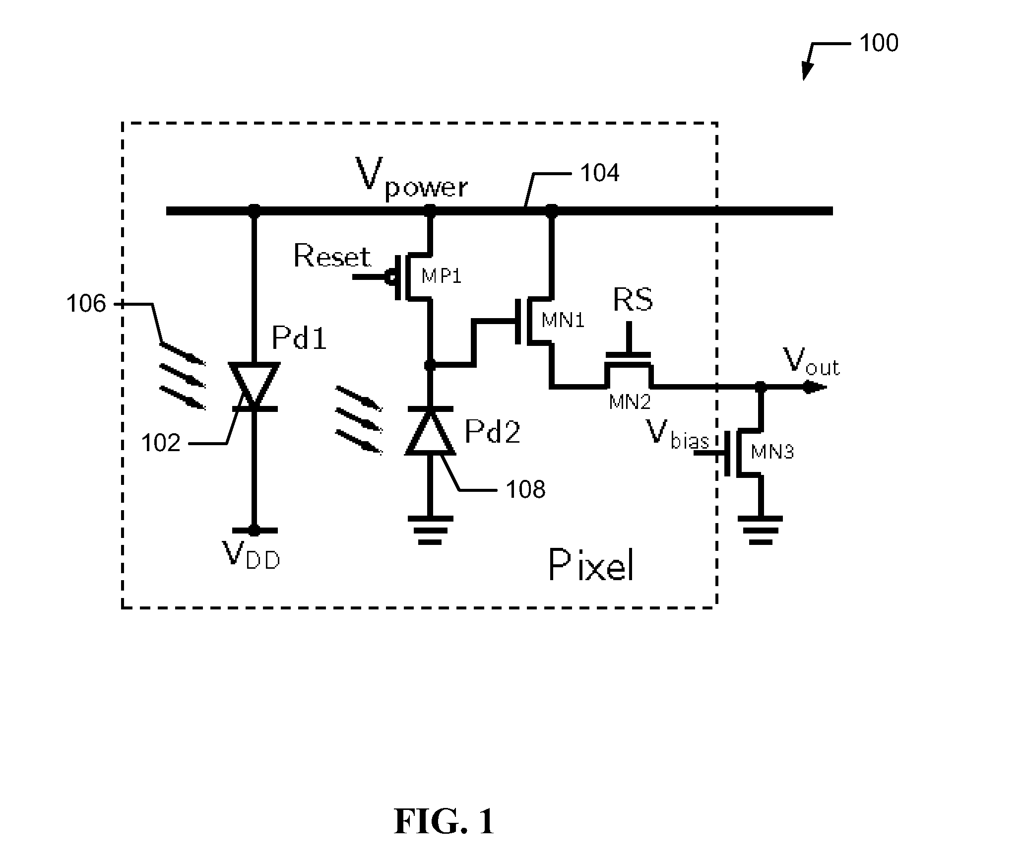
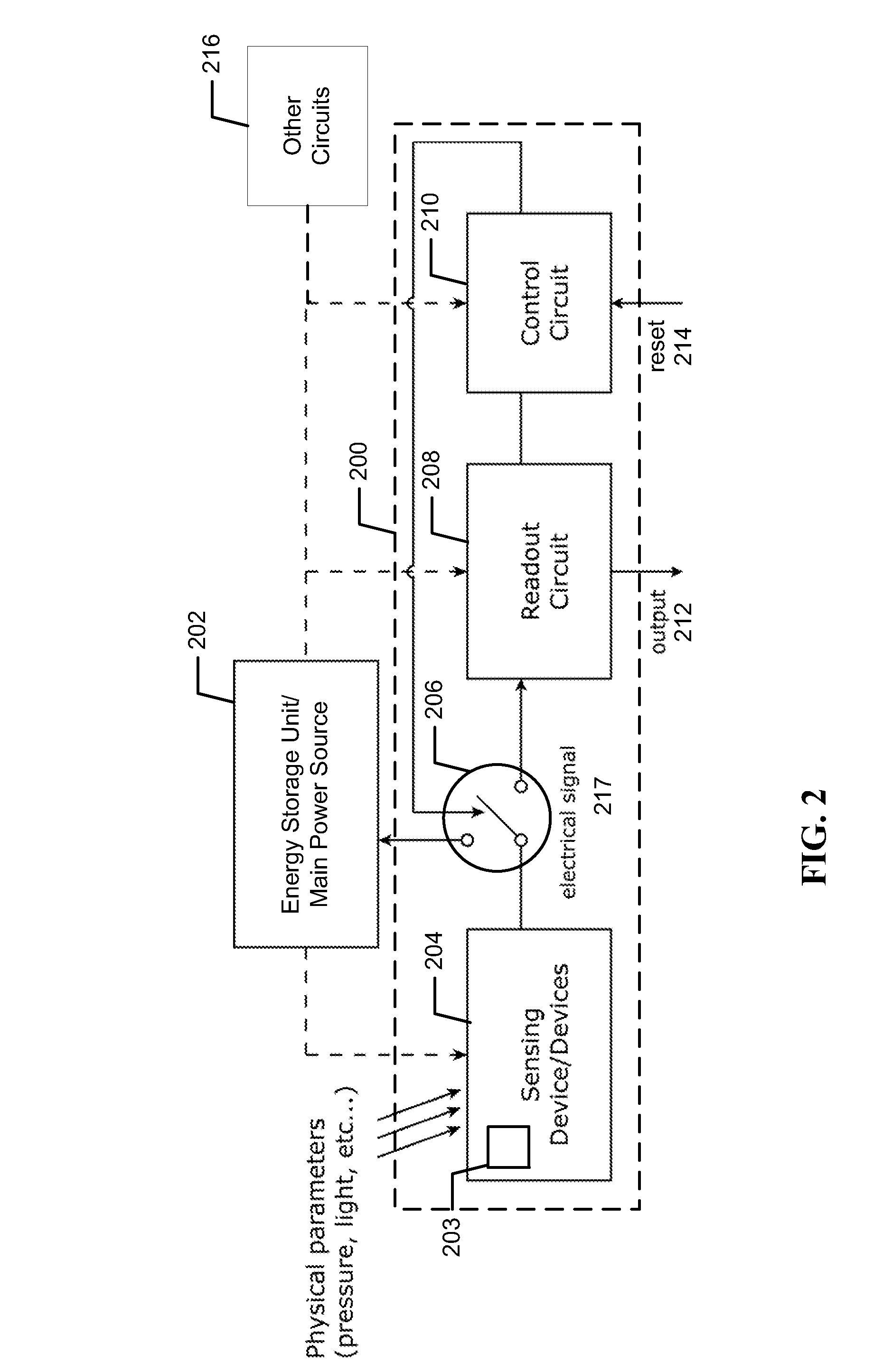
[0022]Now turning to the drawings and referring to FIG. 2, a block diagram is shown therein for illustrating the general structure of circuit 200 for harvesting energy from one or more sensing device 204. The circuit 200, which includes at least one sensing unit 203, can be switched between a sensing mode and a energy harvesting mode. In the sensing mode, the sensing unit 203 converts certain physical parameters or environmental characteristics such as light intensity, pressure, force, acceleration, into output signal 212 which is then readout and digitized. In the energy harvesting mode, the sensing unit 203 is connected to the energy storage unit or main power source 202 to contribute to the power supply, which is used to power various components of the circuit 200 or other external circuit 216.

[0023]As further depicted in FIG. 2, the sensing unit 200 further includes switch 206 for selecting the sensing mode and the energy harvesting mode, a readout circuit 208 for reading and en...


PUM


Abstract

An apparatus using reconfigurable integrated sensor elements with an efficient energy harvesting capability is described. Each sensor element has sensing and energy harvesting mode. In the sensing mode, the sensor element measures an environmental characteristic by generating electrical charge and outputs a time-encoded signal indicative of the measurement. In the energy harvesting mode, the sensor element itself is used to harvest energy from ambient energy source and makes it available to other sensor elements or circuit components. The sensing element is switched from the sensing mode to the energy harvesting mode when the electrical charge reaches a predetermined threshold. An image sensor device using asynchronous readout for harvesting energy from incident light while generating images is also described.

Description

CROSS-REFERENCE TO RELATED APPLICATIONS[0001]This patent application claims the benefit of U.S. Provisional Patent Application No. 61 / 202,435, filed Feb. 27, 2009, which is incorporated by reference in its entirety.FIELD OF THE INVENTION[0002]The present invention relates in general to the fields of electronic sensors and in particular to reconfigurable integrated sensors as both sensing and energy harvesting elements, and to an asynchronous readout technique for efficiently harvesting ambient energy using the sensors.BACKGROUND OF THE INVENTION[0003]Integrated sensors can convert environmental energy into electrical signals, and some of them, as in the case of integrated image sensors, can be used for both sensing and energy harvesting. In the last decade, CMOS image sensors have gained attention due to their inherent advantages of low power and low cost. This is mainly due to the use of standard Complementary Metal Oxide Semiconductor (CMOS) technology which allows for integrating...

Claims


Application Information

Patent Timeline
Patent Type & Authority Patents(United States)
IPC IPC(8): H01L27/00
CPCH04N5/3698H04N5/3741H01L27/14643G01J1/0247G01L1/26G01J1/02G01P15/09G01J1/44G01J1/18G01J1/0228H04N25/709H04N25/766
Inventor BERMAK, AMINESHI, CHAOLAW, MAN KAY
Owner THE HONG KONG UNIV OF SCI & TECH
Why Eureka
Try Eureka