Multilayer wiring board

a multi-layer wiring and mounting board technology, applied in the direction of semiconductor/solid-state device details, electrical apparatus construction details, printed circuit non-printed electric components, etc., can solve the problems of achieving the the transmission of high-frequency signals on the same board, and achieve the suppression of transmission signal degradation, high mounting density, and increase in signal line density

Active Publication Date: 2014-01-21
TOHOKU UNIV +1
View PDF8 Cites 3 Cited by
  • Summary
  • Abstract
  • Description
  • Claims
  • Application Information

AI Technical Summary

Benefits of technology

[0015]According to this invention, while maintaining high mounting density by a first wiring region, it is possible to suppress transmission signal degradation by a second wiring region when a high-frequency signal is transmitted for a long length. Therefore, it is possible to achieve an increase in signal line density and an increase in transmission signal frequency on the same multilayer wiring board.

Problems solved by technology

However, since the propagation loss increases due to the increase in signal frequency and signal line density, it is difficult to ensure the reliability of a transmission signal and thus the problem of achieving the increase in signal line density and the transmission of a high-frequency signal on the same board has not been solved.

Method used


Image

  • Multilayer wiring board
  • Multilayer wiring board
  • Multilayer wiring board

Examples


example 1

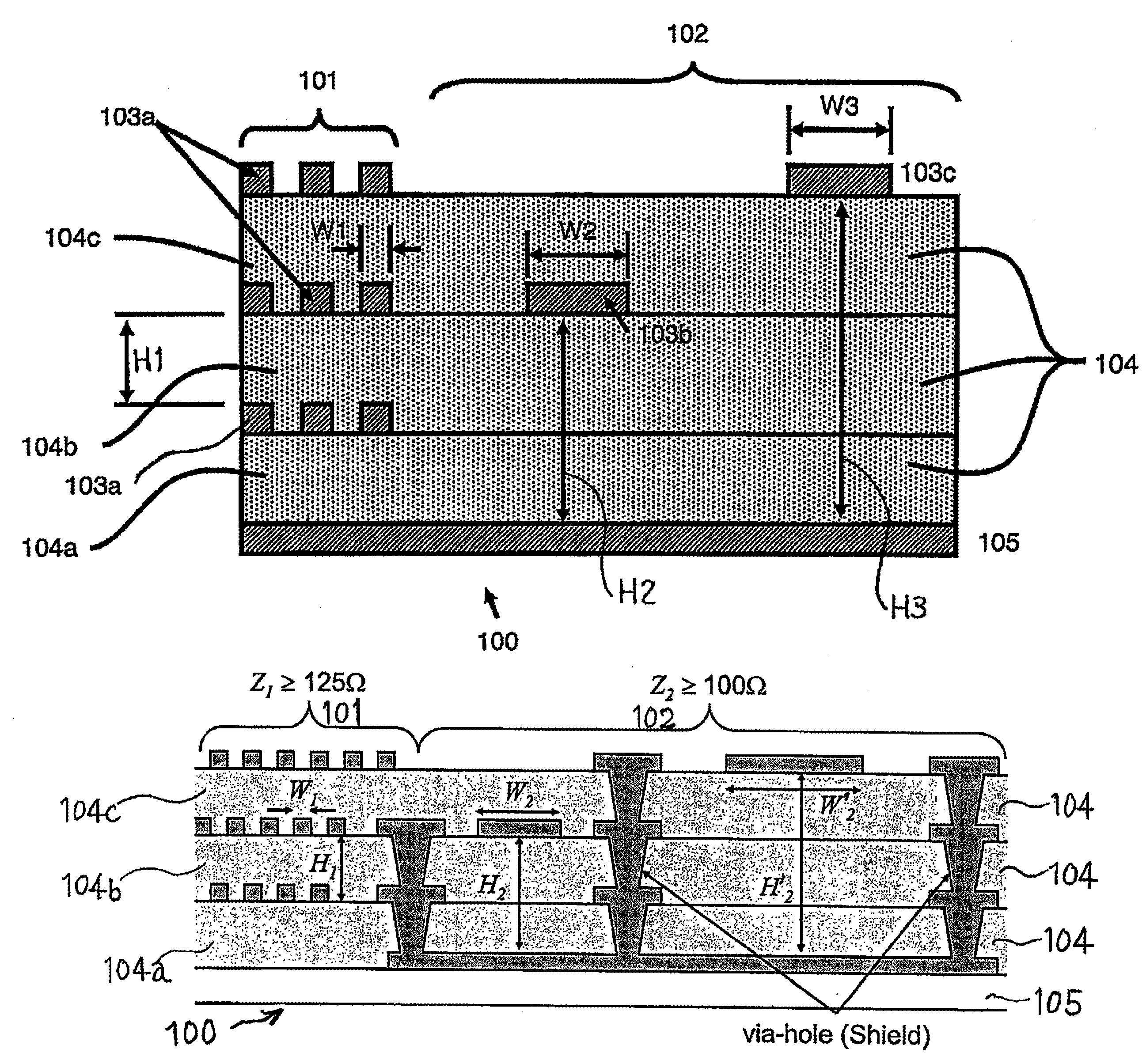
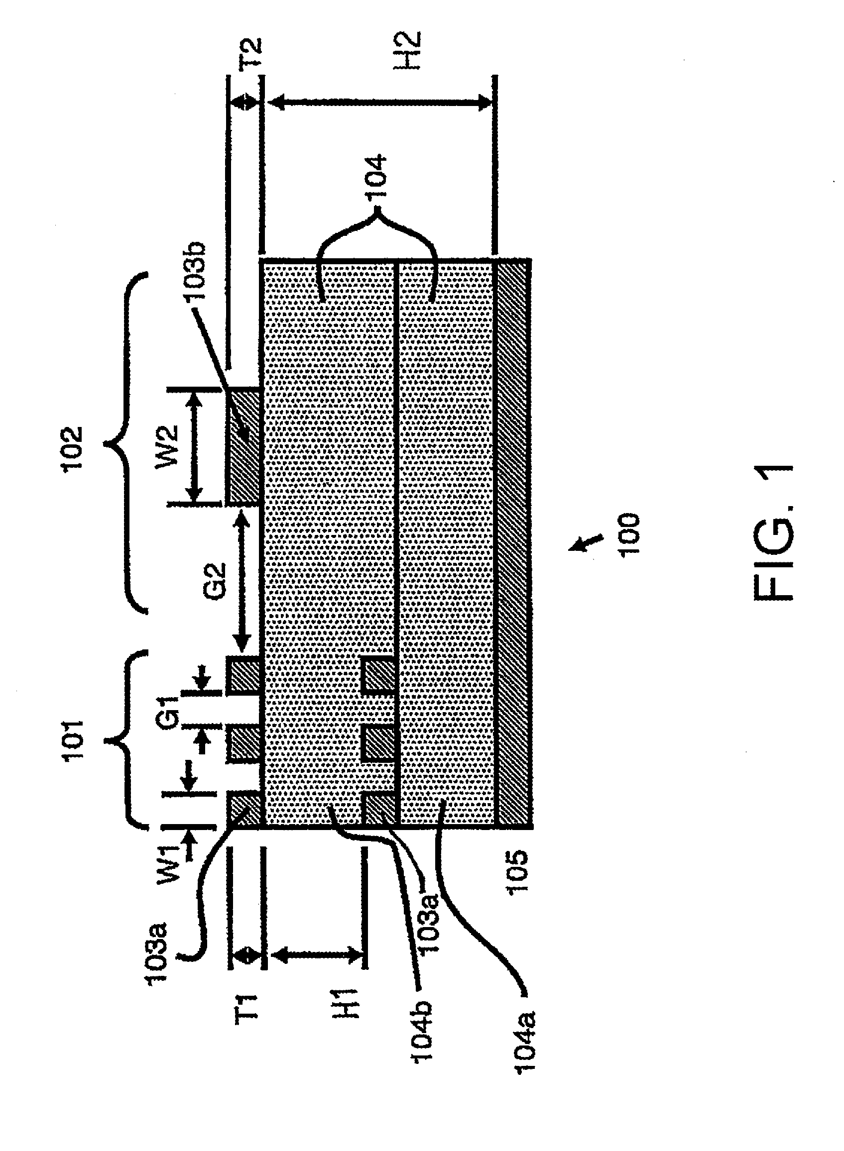
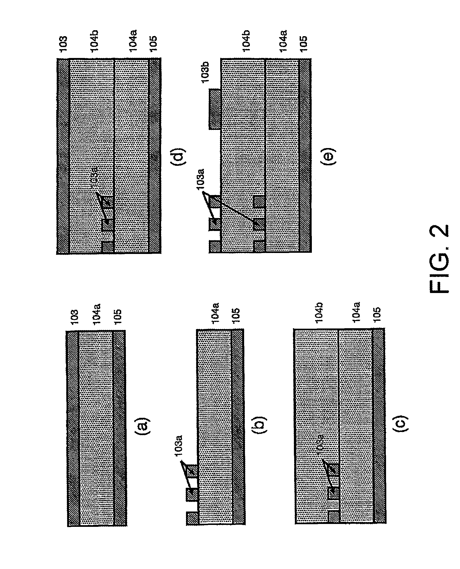
[0059]Referring to FIG. 1, as the first wiring region 101 and the second wiring region 102 each having the multilayer wiring structure described in the above-mentioned first embodiment, a microstrip line structure in which the thickness H1 of the insulating layer 104b was 40 μm, the line width W1 of the wiring 103a was 104 μm, and the line thickness T1 of the wiring 103a was 12 μm and a microstrip line structure in which the thickness H2 of the insulating layer 104 was 80 μm, the line width W2 of the wiring 103b was 215 μm, and the line thickness T2 of the wiring 103b was 12 μm were respectively formed in the same board by the methods described in the above-mentioned first embodiment.

[0060]In this Example 1, the distance G1 between the wirings in the first wiring region 101 was 100 μm while the distance G2 between the wiring 103a in the first wiring region 101 and the wiring 103b in the second wiring region 102 was 150 μm. As the insulating layer 104, use was made of a polycycloolef...

example 2

[0074]Referring to FIG. 10, a description will be given of a multilayer wiring board 100 which is an Example combining the second and third embodiments described with reference to FIGS. 3 and 4. This multilayer wiring board 100 can be called a high-impedance printed wiring board with a plurality of dielectric thicknesses mixed and its structure has, in the single printed wiring board 100, a region that can transmit an ultrahigh-frequency signal in a GHz band, particularly of 10 GHz or more, with a low consumption power, while suppressing a reduction in mounting density to minimum.

[0075]Features of this high-impedance printed wiring board with the plurality of dielectric thicknesses mixed are summarized as follows.

[0076]A) The single printed wiring board 100 has a high-density mounting region 101 for transmitting a low-frequency DC power supply of 1 GHz or less and a high-frequency transmission region 102 that can achieve high-frequency transmission exceeding 1 GHz with a low loss.

[0...


PUM


Abstract

A multilayer wiring board 100 comprises a first wiring region 101 where wirings 103a and insulating layers 104a and 104b are alternately laminated, and a second wiring region 102 where a thickness H2 of an insulating layer 104 is twice or more a thickness H1 of the insulating layer in the first wiring region 101 and a width W2 of a wiring 103b is twice or more a width W1 of the wiring in the first wiring region 101. The first wiring region 101 and the second wiring region 102 are integrally formed on the same board.

Description

[0001]This is a U.S. National Phase Entry of PCT Application No. PCT / JP2009 / 059422, filed May 22, 2009, with a priority date of Jun. 6, 2008, based upon Japanese Patent Application No. 2008-149911.TECHNICAL FIELD[0002]This invention relates to a multilayer wiring board including a board for mounting thereon semiconductor elements such as LSIs or ICs and, in particular, relates to a semiconductor element mounting board and a multilayer wiring board in general that can reduce electrical signal loss in high-frequency application.BACKGROUND ART[0003]A multilayer wiring board is widely used such that it is mounted with semiconductor elements and is, along with the semiconductor elements, accommodated in the same package to form a semiconductor device or such that it is mounted with a plurality of electronic components (semiconductor devices and other active components, passive components such as capacitors and resistance elements, etc.) to form an electronic device such as an information...

Claims


Application Information

Patent Timeline
Patent Type & Authority Patents(United States)
IPC IPC(8): H05K1/03H05K1/11
CPCH01L2223/6616H05K2201/0715H05K1/0218H05K1/0265H05K1/025H01L2924/19032H05K2201/09727H01L2924/0002H05K2201/09972H01L2223/6688H01L2223/6627H01L2924/3011H05K2201/09618H01L23/66H05K2201/0191H05K2201/0352H05K3/4652H05K2201/096H01L2924/00
Inventor OHMI, TADAHIROSUGAWA, SHIGETOSHIIMAI, HIROSHITERAMOTO, AKINOBU
Owner TOHOKU UNIV
Why Eureka
Try Eureka