MR sensor with flux guide enhanced hard bias structure
a technology of hard bias structure and flux guide, which is applied in the field of mr sensor fabrication, can solve the problems of affecting the reading process of high density magnetic recording, less effective at orienting the free layer magnetization, and increasing the noise produced by the sensor, so as to reduce the magnetostatic coupling, promote crystalline anisotropy, and reduce the effect of coercivity
- Summary
- Abstract
- Description
- Claims
- Application Information
AI Technical Summary
Benefits of technology
Problems solved by technology
Method used
Image
Examples
embodiment 1
[0051]In what follows, for ease and consistency of description, laterally directed dimensions (in the ABS plane) will be denoted “widths,” vertically directed dimensions (in the ABS plane) will be denoted “thicknesses” and dimensions directed from the ABS plane of the sensor towards the backside will be denoted “depths.” If other terms are utilized, they will be defined as needed. For example, the depth direction will sometimes be referred to as the “stack height.”
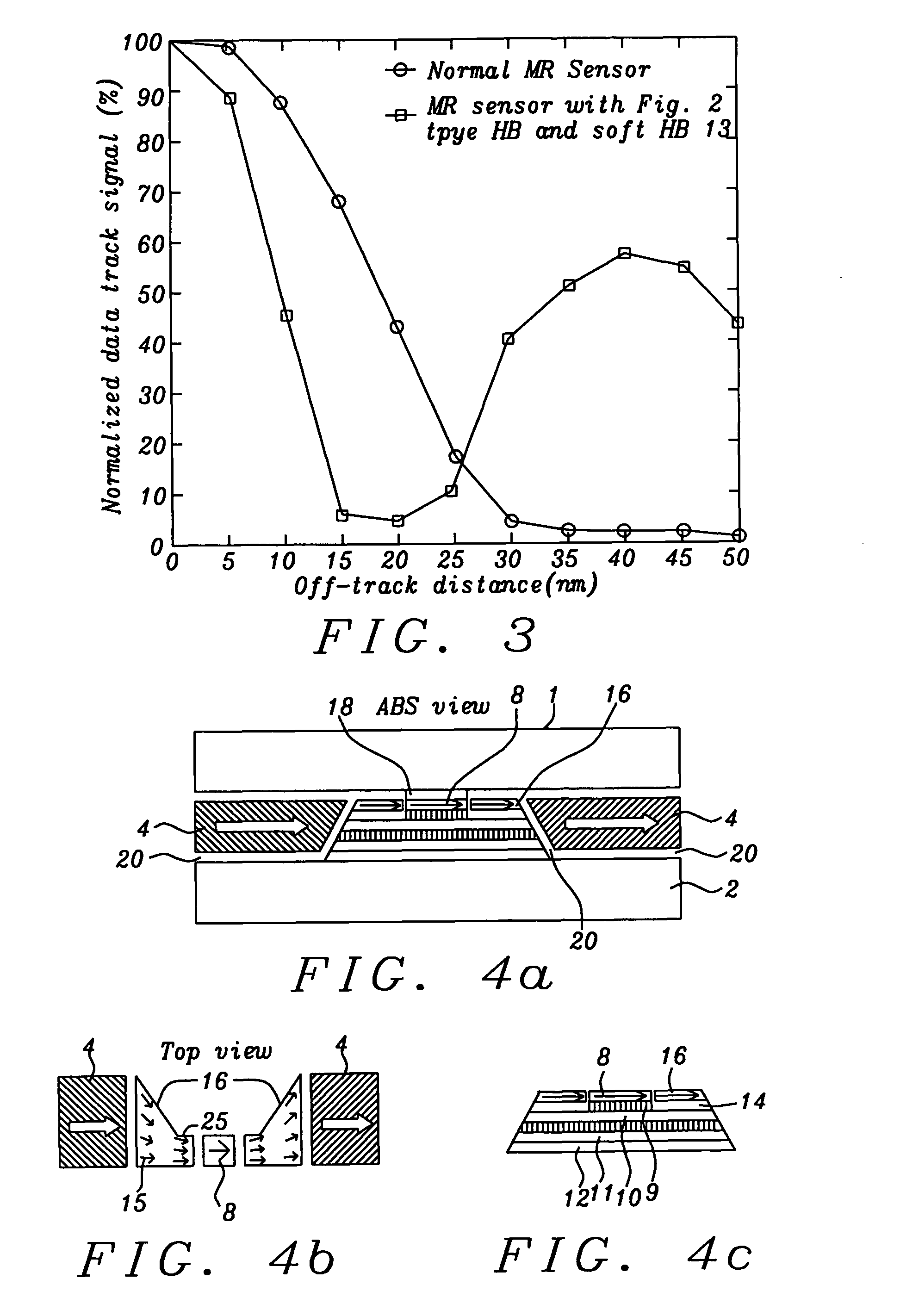
[0052]Referring now to schematic FIGS. 4a, 4b and 4c, there is shown, first, in FIG. 4a, an ABS view of a first embodiment of the present invention. Reader shields (1) (top or upper shield) and (2) (bottom shield) are formed above and below the CPP MR sensor stack (6) that is patterned to accept the short substantially vertical edges of the flux guides (16) on either side of the substantially vertical edges free layer (8). The sensor stack is a vertical lamination of horizontal layers that will be described below. The read...
embodiment 2
[0067]Referring now to schematic FIGS. 8a, 8b and 8c, there is shown, first, in FIG. 8a, an ABS view of a second embodiment of the present invention, in FIG. 8b there is shown a top view (cross-section between the shields) of FIG. 8a and in FIG. 8c there is shown a more detailed view of the sensor stack (6) components and the positioning of the FG layer (16) and its magnetization vectors (arrows).
[0068]Reader shields (1) (top or upper shield) and (2) (bottom shield) are formed above and below (RSS separation approximately 10 to 40 nm) the CPP MR sensor stack (6) that is patterned to accept the short edges of the flux guides (FG) (16) on the etched slopes of the sensor stack. These etched slopes can extend through more than two layers of the MR stack. It is noted that the width of the free layer (8) is between approximately 10 and 100 nm and the widths of the layers (9)-(12) below the free layer are greater, corresponding to the slope of the sides. Unlike the patterned shape of FIG. ...
PUM
 Abstract
Description
Claims
Application Information


