Techniques for metal gate workfunction engineering to enable multiple threshold voltage FINFET devices

a technology of gate work and function engineering, applied in the field of gate work function engineering, can solve the problems of multiple threshold voltage (vt) devices, aggressively scaled devices have serious drawbacks, and require a substantial amount of process complexity

Active Publication Date: 2014-03-11
GLOBALFOUNDRIES US INC
View PDF18 Cites 48 Cited by
  • Summary
  • Abstract
  • Description
  • Claims
  • Application Information

AI Technical Summary

Problems solved by technology

One key problem with undoped devices is the implementation of multiple threshold voltage (Vt) devices.
To do so, however, for aggressively scaled devices has serious drawbacks from random dopant fluctuation (RDF) effects.
This however requires a substantial amount of process complexity.

Method used


Image

  • Techniques for metal gate workfunction engineering to enable multiple threshold voltage FINFET devices
  • Techniques for metal gate workfunction engineering to enable multiple threshold voltage FINFET devices
  • Techniques for metal gate workfunction engineering to enable multiple threshold voltage FINFET devices

Examples


example

14 nm SOI FIN FET

[0044]Exemplary device dimensions are provided in FIG. 12. Exemplary Fin width values range from about 6 nm to about 14 nm, Fin Height values range from about 15 nm to about 30 nm, and Fin Pitch values range from about 20 nm to about 60 nm. For an exemplary fin width of 12 nm, Fin Height of 27 nm, Fin Pitch of 40 nm, interfacial oxide thickness of 1 nm, and hi-k dielectric thickness of 2 nm, and a gate metal thickness of 2 nm, the trench in which gate work function engineering occurs is 18 nm wide and 27 nm tall, yielding an aspect ratio of 1:1.5. Thus, work function modulation could be achieved using a CVD process which deposits differently in trenches with aspect ratios of, for example, 1:1, 1:1.5, and 1:2 by increasing the fin pitch to 49 nm for some devices and decreasing the fin pitch to 35.5 nm for other devices.

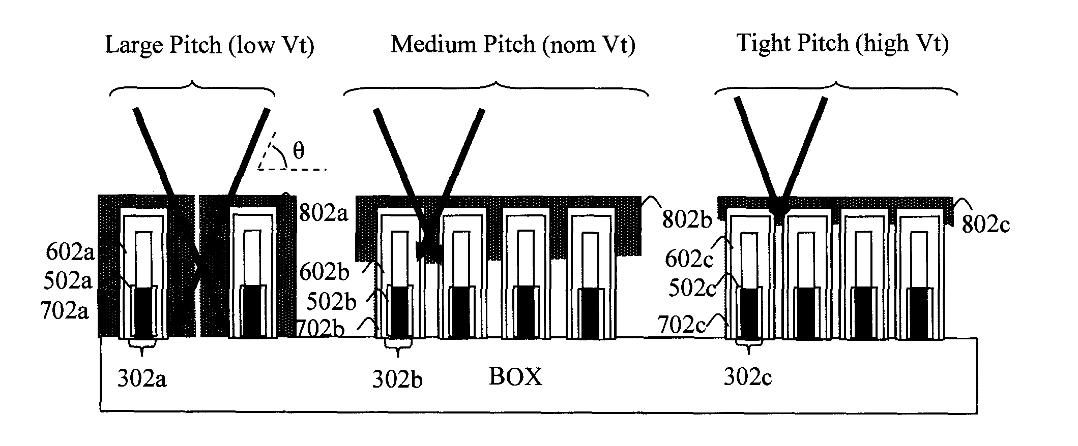
[0045]In another embodiment, an angled evaporation approach could be used to modulate thickness of work function setting material on the fins. As illu...


PUM


Abstract

Techniques are provided for gate work function engineering in FIN FET devices using a work function setting material an amount of which is provided proportional to fin pitch. In one aspect, a FIN FET device is provided. The FIN FET device includes a SOI wafer having an oxide layer and a SOI layer over a BOX, and a plurality of fins patterned in the oxide layer and the SOI layer; an interfacial oxide on the fins; and at least one gate stack on the interfacial oxide, the gate stack having (i) a conformal gate dielectric layer present, (ii) a conformal gate metal layer, and (iii) a conformal work function setting material layer. A volume of the conformal gate metal layer and a volume of the conformal work function setting material layer present in the gate stack is proportional to a pitch of the fins.

Description

CROSS-REFERENCE TO RELATED APPLICATION(S)[0001]This application is a continuation of U.S. application Ser. No. 13 / 596,687 filed on Aug. 28, 2012, the disclosure of which is incorporated by reference herein.FIELD OF THE INVENTION[0002]The present invention relates to FIN field-effect transistor (FET) devices, and more particularly, to techniques for gate work function engineering using a work function setting material an amount of which is provided proportional to fin pitch so as to enable multiple threshold voltage devices.BACKGROUND OF THE INVENTION[0003]In current complementary metal-oxide semiconductor (CMOS) scaling, the use of undoped FIN field-effect transistor (FET) devices is highly preferred as a device choice for CMOS at and beyond the 22 nanometer (nm) node. One key problem with undoped devices is the implementation of multiple threshold voltage (Vt) devices. One solution is to dope the FINFET device. To do so, however, for aggressively scaled devices has serious drawback...

Claims


Application Information

Patent Timeline
Patent Type & Authority Patents(United States)
IPC IPC(8): H01L27/092
CPCH01L27/1211H01L21/845
Inventor CHANG, JOSEPHINE B.LAUER, ISAACLIN, CHUNG-HSUNSLEIGHT, JEFFREY W.
Owner GLOBALFOUNDRIES US INC
Why Eureka
Try Eureka