Ultra-thin copper foil with carrier and copper-clad laminate board or printed circuit board substrate
a technology of printed circuit board and copper foil, which is applied in the direction of carbon-silicon compound conductors, conductors, transportation and packaging, etc., can solve the problems of mechanical strength, tearing of copper foil, and ruined verticality of the side walls of interconnect patterns formed, etc., to achieve easy peeling of carrier foil, stable in carrier peeling, and resistance to blistering
- Summary
- Abstract
- Description
- Claims
- Application Information
AI Technical Summary
Benefits of technology
Problems solved by technology
Method used
Image
Examples
examples
[0071]Below, the present invention will be more specifically explained using examples.
[0072]The plating conditions of the examples are shown in Table 1.
[0073]
TABLE 1Plating ConditionsCurrentName ofConcentrationdensityTemperaturePlating typechemical(g / L)(A / dm2)(° C.)pHCu platingCu2P2O7•3H2O3 to 500.1 to 5 20 to 60 8 to 11condition 1K4P2O750 to 350Cu platingCu2P2O7•3H2O10 to 150 1 to 1020 to 60 8 to 12condition 2K4P2O750 to 400NH3OH (28%) 1 to 10 mL / LCu platingCopper10 to 70 1 to 6010 to 701 to 2condition 3sulfate (asCu metal)Sulfuric30 to 120acidNi platingNickel 1 to 120 1 to 6010 to 703 to 5sulfate(as Ni)Boric acid10 to 50 Mo—Co platingCo amount0.1 to 20 0.1 to 6010 to 703 to 5Mo amount0.05 to 20 Citric acid 5 to 240Mo—NiNi sulfate10 to 1000.5 to 1510 to 50 8 to 11platinghexahydrateSodium10 to 100molybdatedihydrateSodium30 to 200citrateW—NiNi sulfate10 to 1000.5 to 1530 to 907 to 8platinghexahydrateSodium10 to 100tungstatedihydrateSodium30 to 200citrate
examples 1 to 8
[0074]Production of ultra-thin copper foils with carriers by carrier foil→Mo—Co plating (first release layer)→Mo—Co plating (second release layer)→copper strike plating→copper plating (ultra-thin copper foil).
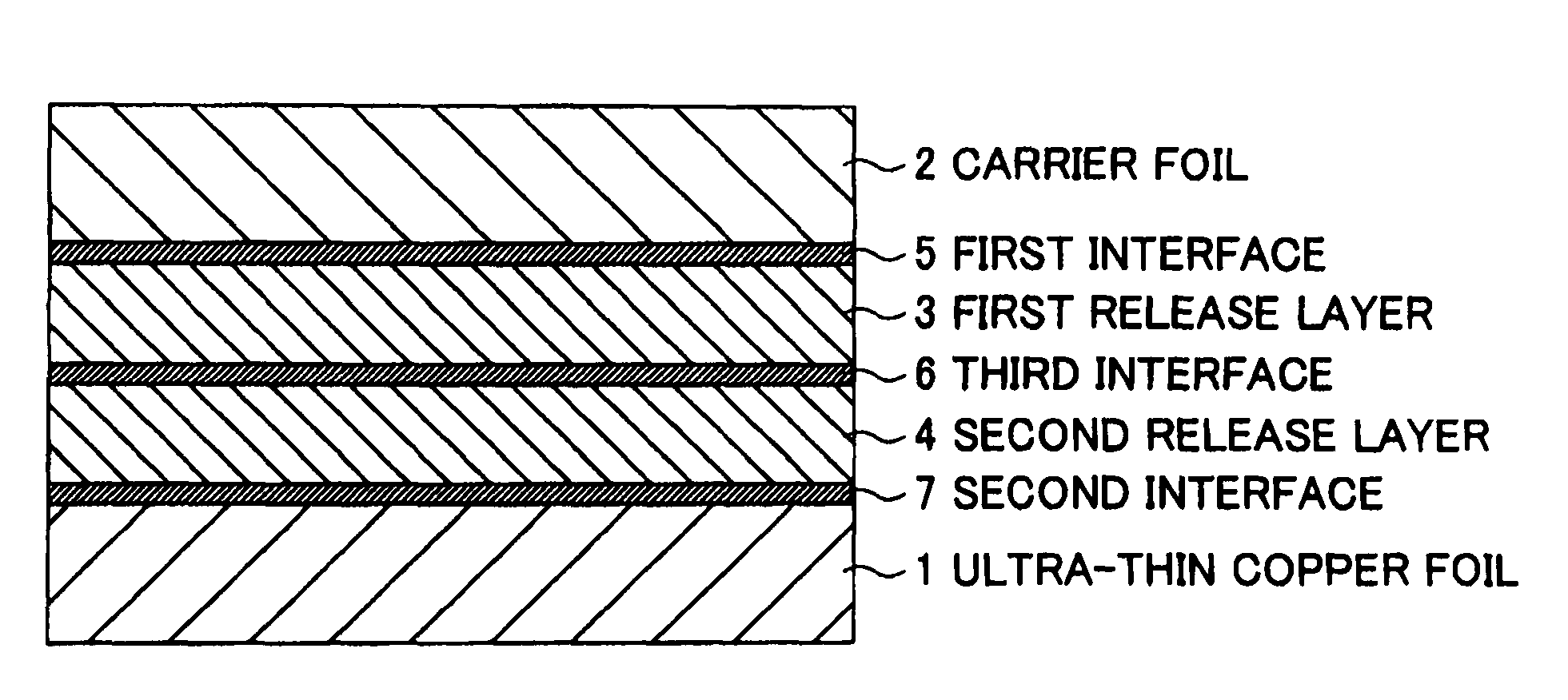
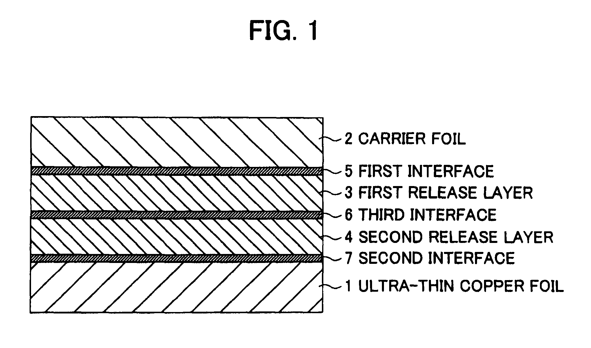
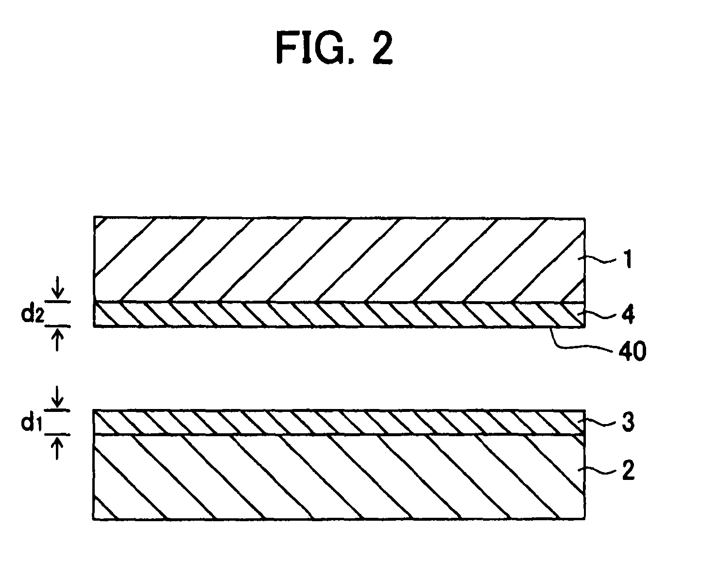
[0075]A copper foil (thickness: 31 μm) having an Rz of 0.8 μm at one surface was used as the carrier foil. A first release layer was formed on the carrier foil by Mo—Co plating in a first plating bath under the described in Table 1. After transfer from the first plating bath to the second plating bath, the second release layer was formed by the Mo—Co plating in the second plating bath. During the transfer from the first plating bath to the second plating bath, a third interface was formed on the surface of the first release layer. By suitably adjusting the formation time of this first release layer or second release layer, the release layers of Examples 1 to 8 were formed.
[0076]Then, onto this second release layer, copper strike plating was applied under the above to a thickn...
example 9
[0078]Except for dipping the sample into the following oxidizing treatment solution during the transfer from the first plating bath to the second plating bath, the same treatment was performed as in Examples 1 to 8 to obtain an ultra-thin copper foil with a carrier.
[0079]Sulfuric acid: 10 to 30 g / dm3
[0080]Hydrogen peroxide solution: 30 to 60 g / dm3
[0081]Bath temperature: 10 to 30° C.
PUM
| Property | Measurement | Unit |
|---|---|---|
| temperature | aaaaa | aaaaa |
| thickness | aaaaa | aaaaa |
| thickness | aaaaa | aaaaa |
Abstract
Description
Claims
Application Information


