Ultra-thin copper foil with carrier and copper-clad laminate board or printed circuit board substrate

a technology of printed circuit board and copper foil, which is applied in the direction of transportation and packaging, layered products, chemical instruments and processes, etc., can solve the problems of mechanical strength, tearing of copper foil, and ruined verticality of the side walls of interconnect patterns formed, etc., to achieve easy peeling of carrier foil, stable in carrier peeling, and resistance to blistering

Active Publication Date: 2011-09-01
FURUKAWA ELECTRIC CO LTD
View PDF14 Cites 17 Cited by
  • Summary
  • Abstract
  • Description
  • Claims
  • Application Information

AI Technical Summary

Benefits of technology

[0035]The present invention can provide an ultra-thin copper foil with a carrier which is stable in carrier peel, is resistant to blistering, and enables easy peeling of the carrier foil from the ultra-thin copper foil even under a high temperature environment.
[0036]Further, the present invention can provide a copper-clad laminate board substrate or printed circuit board substrate which becomes the base of a printed circuit board, multilayer printed circuit board, chip-on-film-use circuit board etc. for fine pattern applications using the ultra-thin copper foil with a carrier.

Problems solved by technology

As a result, the verticality of the side walls of the interconnect patterns formed is ruined.
However, such 9 μm or less thin copper foil (hereinafter, sometimes referred to as an “ultra-thin copper foil”) is weak in mechanical strength, easily suffers from wrinkles or creases at the time of production of the printed circuit board substrate, and sometimes causes tearing of the copper foil.
When peeling off of the carrier foil after hot bonding the ultra-thin copper foil to the resin base material, the problem arises of deformation of the ultra-thin copper foil if the ultra-thin copper foil has a thickness less than 5 μm.
However, in a circuit board substrate using a polyimide or other highly heat resistant resin as the resin base material, a heating temperatures when pressing the copper foil and a resin and curing the resin becomes high.
This cannot be handled by an organic-based release layer where peeling becomes difficult due to a rise of the peeling strength caused by this heat treatment, so a metal-based release layer is mainly being used.
However, due to differences of the ratio of the oxide content and thickness of the oxide coating film, there were the problems that variations easily arose in the carrier peel, the carrier peel was hard to stabilize, and blistering occurred.
Further, at the surface of oxides, precipitation by electroplating of copper is hard to occur, so it is difficult to uniformly plate the release layer.
Therefore, sometimes there also arise the problems of variation of thickness of the ultra-thin copper foil and occurrence of pinholes.
However, since the interface at which peeling is liable to occur does not become constant, the problem of the carrier peel becoming higher and harder to stabilize could not be solved.

Method used


Image

  • Ultra-thin copper foil with carrier and copper-clad laminate board or printed circuit board substrate
  • Ultra-thin copper foil with carrier and copper-clad laminate board or printed circuit board substrate
  • Ultra-thin copper foil with carrier and copper-clad laminate board or printed circuit board substrate

Examples


examples

[0072]Below, the present invention will be more specifically explained using examples.

[0073]The plating conditions of the examples are shown in Table 1.

TABLE 1Plating ConditionsCurrentName ofConcentrationdensityTemperaturePlating typechemical(g / L)(A / dm2)(° C.)pHCu platingCu2P2O7•3H2O3 to 500.1 to 5 20 to 60 8 to 11condition 1K4P2O750 to 350Cu platingCu2P2O7•3H2O10 to 150  1 to 1020 to 60 8 to 12condition 2K4P2O750 to 400NH3OH (28%)    1 to 10 mL / LCu platingCopper10 to 70   1 to 6010 to 701 to 2condition 3sulfate (asCu metal)Sulfuric30 to 120acidNi platingNickel 1 to 120  1 to 6010 to 703 to 5sulfate(as Ni)Boric acid10 to 50 Mo—Co platingCo amount0.1 to 20  0.1 to 6010 to 703 to 5Mo amount0.05 to 20  Citric acid 5 to 240Mo—NiNi sulfate10 to 1000.5 to 1510 to 50 8 to 11platinghexahydrateSodium10 to 100molybdatedihydrateSodium30 to 200citrateW—NiNi sulfate10 to 1000.5 to 1530 to 907 to 8platinghexahydrateSodium10 to 100tungstatedihydrateSodium30 to 200citrate

examples 1 to 8

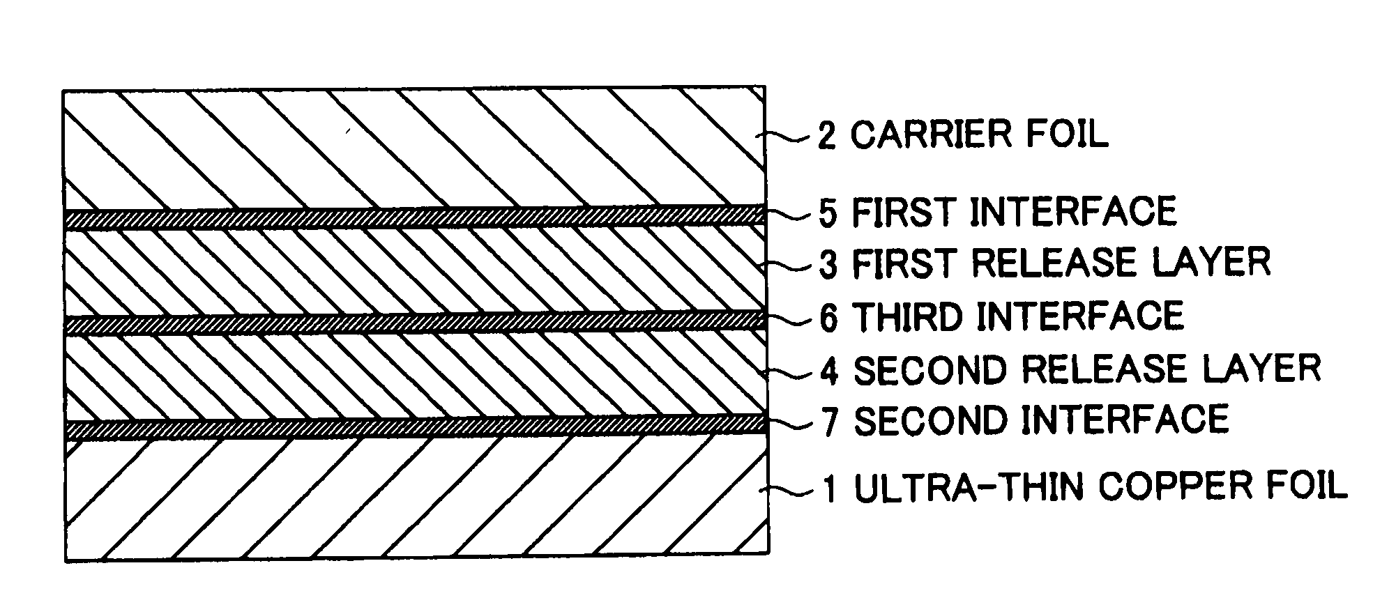
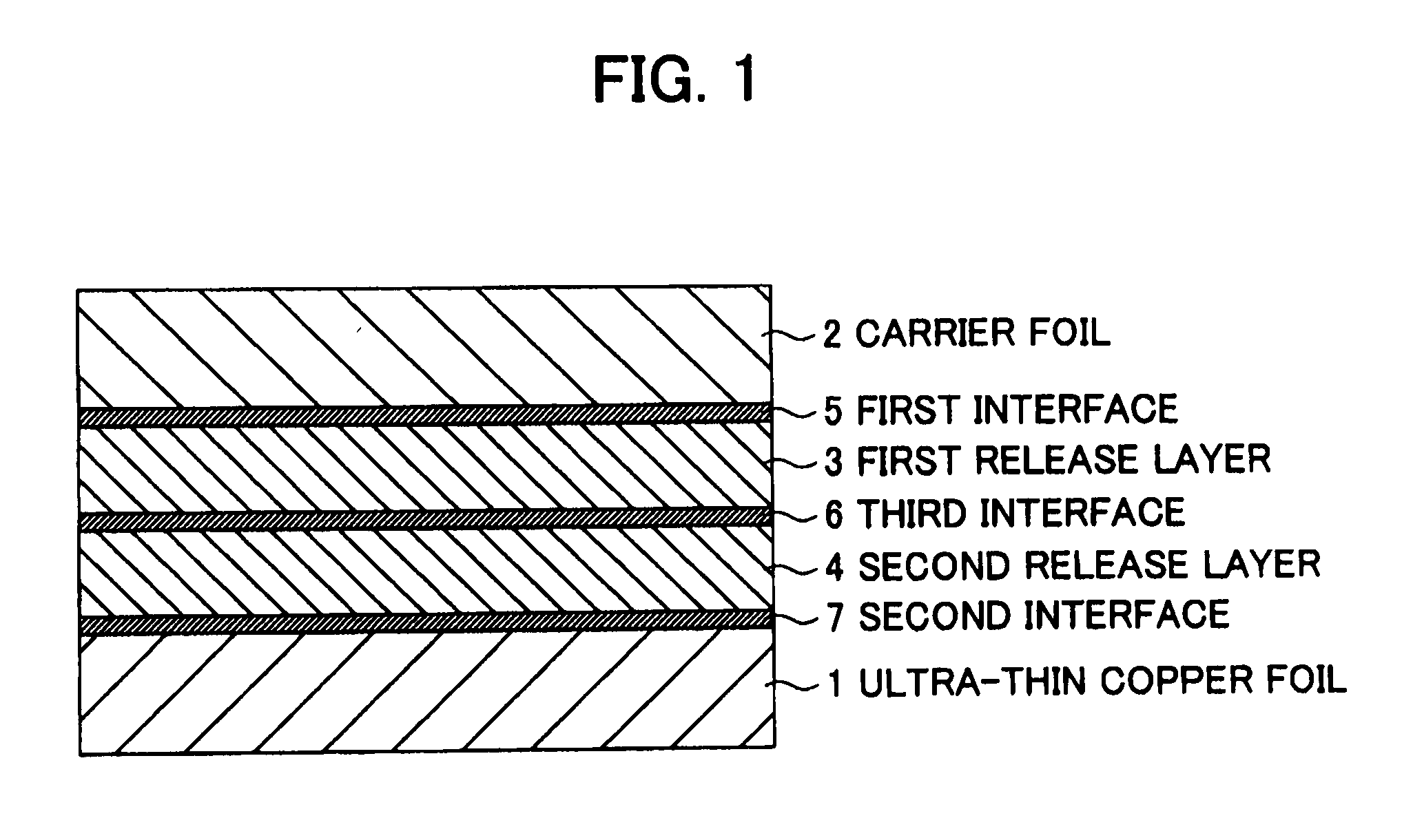
[0074]Production of ultra-thin copper foils with carriers by carrier foil→Mo—Co plating (first release layer)→Mo—Co plating (second release layer)→copper strike plating→copper plating (ultra-thin copper foil).

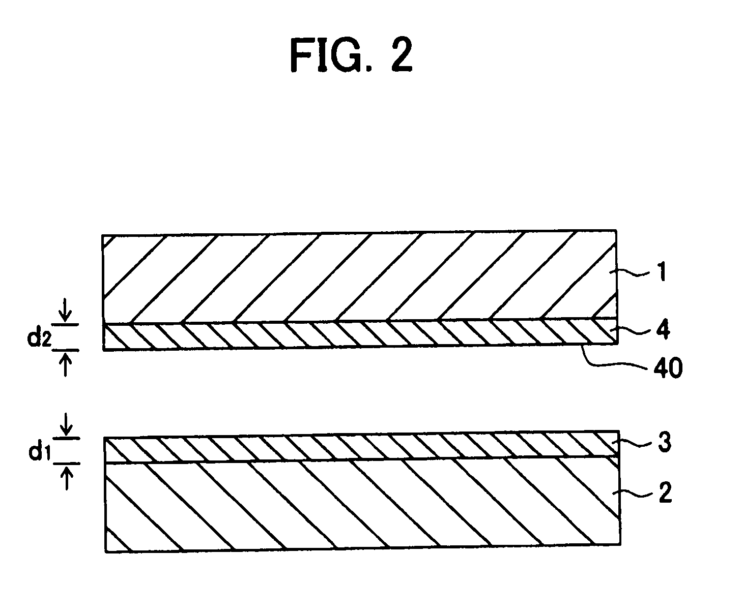
[0075]A copper foil (thickness: 31 μm) having an Rz of 0.8 μm at one surface was used as the carrier foil. A first release layer was formed on the carrier foil by Mo—Co plating in a first plating bath under the described in Table 1. After transfer from the first plating bath to the second plating bath, the second release layer was formed by the Mo—Co plating in the second plating bath. During the transfer from the first plating bath to the second plating bath, a third interface was formed on the surface of the first release layer. By suitably adjusting the formation time of this first release layer or second release layer, the release layers of Examples 1 to 8 were formed.

[0076]Then, onto this second release layer, copper strike plating was applied under the above to a thickn...

example 9

[0078]Except for dipping the sample into the following oxidizing treatment solution during the transfer from the first plating bath to the second plating bath, the same treatment was performed as in Examples 1 to 8 to obtain an ultra-thin copper foil with a carrier.

[0079]Sulfuric acid: 10 to 30 g / dm3

[0080]Hydrogen peroxide solution: 30 to 60 g / dm3

[0081]Bath temperature: 10 to 30° C.


PUM

PropertyMeasurementUnit
temperatureaaaaaaaaaa
thicknessaaaaaaaaaa
thicknessaaaaaaaaaa

Abstract

The invention has as its object to provide an ultra-thin copper foil with a carrier which suppresses occurrence of blistering and is stable in peeling strength, in particular provides an ultra-thin copper foil with a carrier enabling easy peeling of a carrier foil from an ultra-thin copper foil even under a high temperature environment. As means for that, there is provided an ultra-thin copper foil with a carrier comprised of a carrier foil, a release layer, and a copper foil, wherein the release layer is formed by a first release layer disposed on the carrier foil side and a second release layer disposed on the ultra-thin copper foil side, there is a first interface between the carrier foil and the first release layer, a second interface between the ultra-thin copper foil and the second release layer, and a third interface between the first release layer and the second release layer, and the peeling strengths at the interfaces are first interface>third interface, and second interface>third interface.

Description

TECHNICAL FIELD[0001]The present invention relates to an ultra-thin copper foil with a carrier and to a printed circuit board substrate which uses the ultra-thin copper foil with a carrier, more particularly relates to an ultra-thin copper foil with a carrier suitable for use at a high temperature of 300° C. or more and to a circuit board using the ultra-thin copper foil.BACKGROUND ART[0002]Usually, a copper foil which is used for a printed circuit board substrate which forms the base of a printed circuit board, multilayer printed circuit board, chip-on-film-use circuit board, etc. is roughened at its surface on the side to be hot bonded to a resin substrate or the like. This roughened surface exhibits an anchoring effect for the substrate. This thereby raises the bond strength between the substrate and the copper foil to secure reliability as the printed circuit board substrate.[0003]In recent years, in circuit boards, to deal with the high integration of various types of electroni...

Claims


Application Information

Patent Timeline
Patent Type & Authority Applications(United States)
IPC IPC(8): H05K1/03B32B15/04B32B7/02
CPCC25D5/12B32B15/01C25D3/38C25D1/20B32B15/08C22C9/00Y10T428/2495H05K2203/0315B32B15/20C25D1/04C25D5/48H05K3/025Y10T428/31678C25D7/06H05K3/00
Inventor UNO, TAKEOKAWAKAMI, AKIRASUZUKI, YUJI
Owner FURUKAWA ELECTRIC CO LTD
Why Eureka
Try Eureka