
Optical linear feedback circuit

a feedback circuit and linear feedback technology, applied in logic circuits using specific components, pulse techniques, instruments, etc., can solve the problems of increasing in-band ase noise, weak equalization between bits in the sequence and the quality of pulses, and limiting the number of times that signals can be recirculated, so as to achieve easy and cheaper construction, design and manufacturing. the effect of simple structur

Inactive Publication Date: 2014-04-15
TELEFON AB LM ERICSSON (PUBL)
View PDF10 Cites 6 Cited by
  • Summary
  • Abstract
  • Description
  • Claims
  • Application Information

AI Technical Summary

Benefits of technology

The patent describes a new way to build circuits that can shift data using less hardware than previous methods. This is achieved by recirculating the data around a loop delay path, which allows for longer sequences to be built up without needing extra storage cells. This design results in less complicated and expensive manufacturing compared to previous methods.

Problems solved by technology

The number of times that the signals can be recirculated may be limited in practice by noise building up in the loop or by a build up of differences in power levels of the parts of the sequence.
The equalization between bits in the sequence and the quality of the pulses is strongly limited by the accumulating ASE noise inside the buffer, the long fiber-based structure and the bit's polarization.
As the packet circulates in the buffer, the added in-band ASE noise increases every round trip, reducing the extinction ratio and the efficiency of all the processes afterward.
The fiber-based setup also can cause misalignment between the clocks, spoil the essential synchronism and degrade the performance of the FWM and the XOR operation.

Method used


Image

  • Optical linear feedback circuit
  • Optical linear feedback circuit
  • Optical linear feedback circuit

Examples


Embodiment Construction

[0018]The present invention will be described with respect to particular embodiments and with reference to certain drawings but the invention is not limited thereto but only by the claims. The drawings described are only schematic and are non-limiting. In the drawings, the size of some of the elements may be exaggerated and not drawn on scale for illustrative purposes.

DEFINITIONS

[0019]Where the term “comprising” is used in the present description and claims, it does not exclude other elements or steps. Where an indefinite or definite article is used when referring to a singular noun e.g. “a” or “an”, “the”, this includes a plural of that noun unless something else is specifically stated.

[0020]The term “comprising”, used in the claims, should not be interpreted as being restricted to the means listed thereafter; it does not exclude other elements or steps.

[0021]References to nodes can encompass any kind of switching node, not limited to the types described, not limited to any level o...


PUM

PropertyMeasurementUnit
wavelengthaaaaaaaaaa
optical power lossesaaaaaaaaaa

Abstract

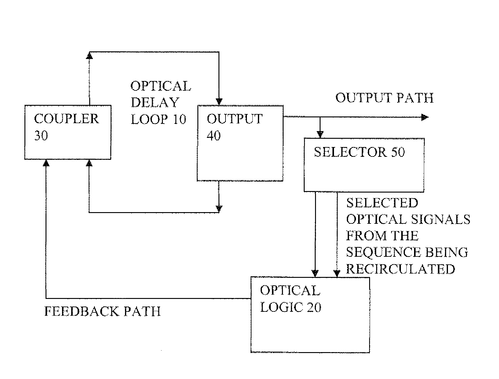
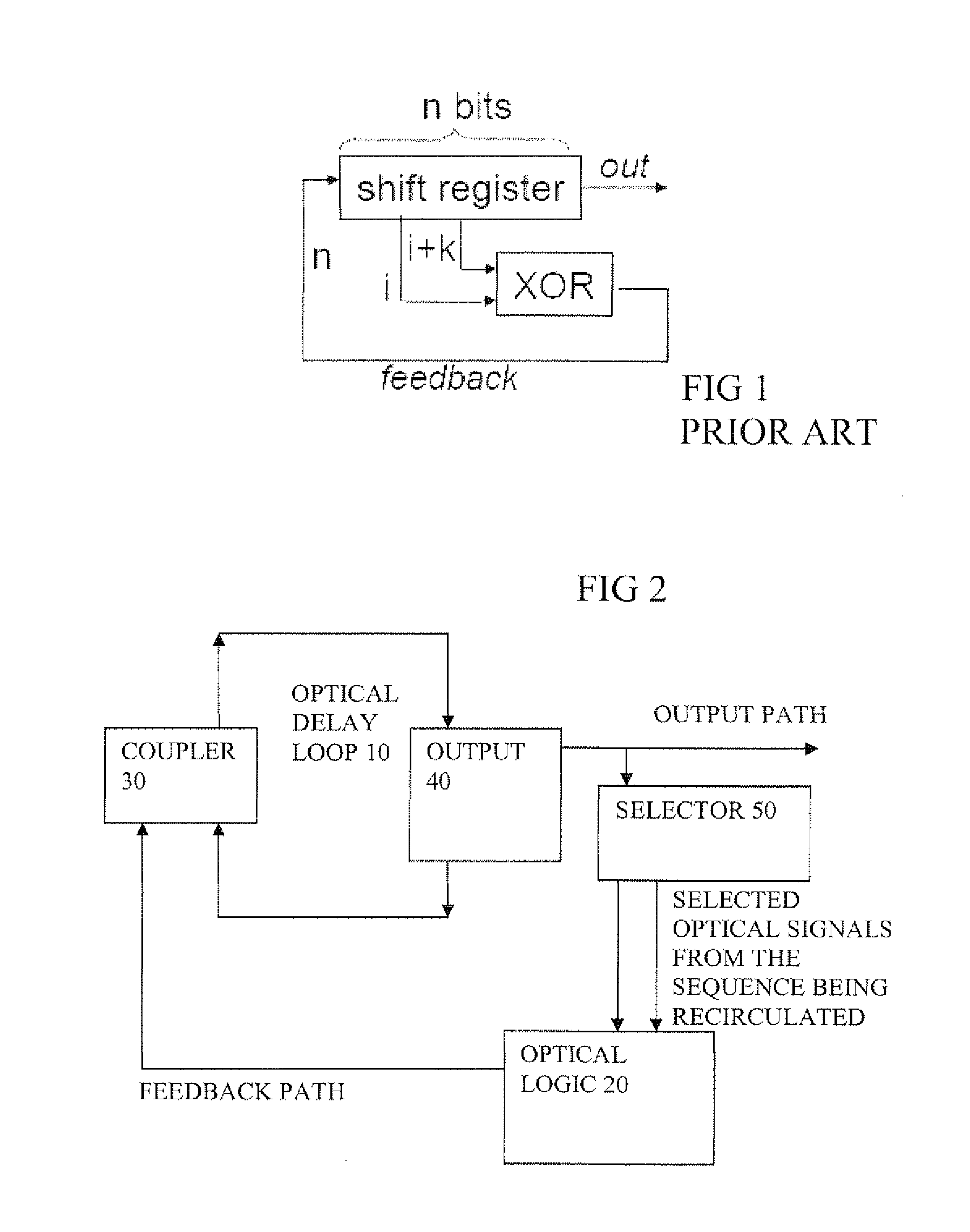
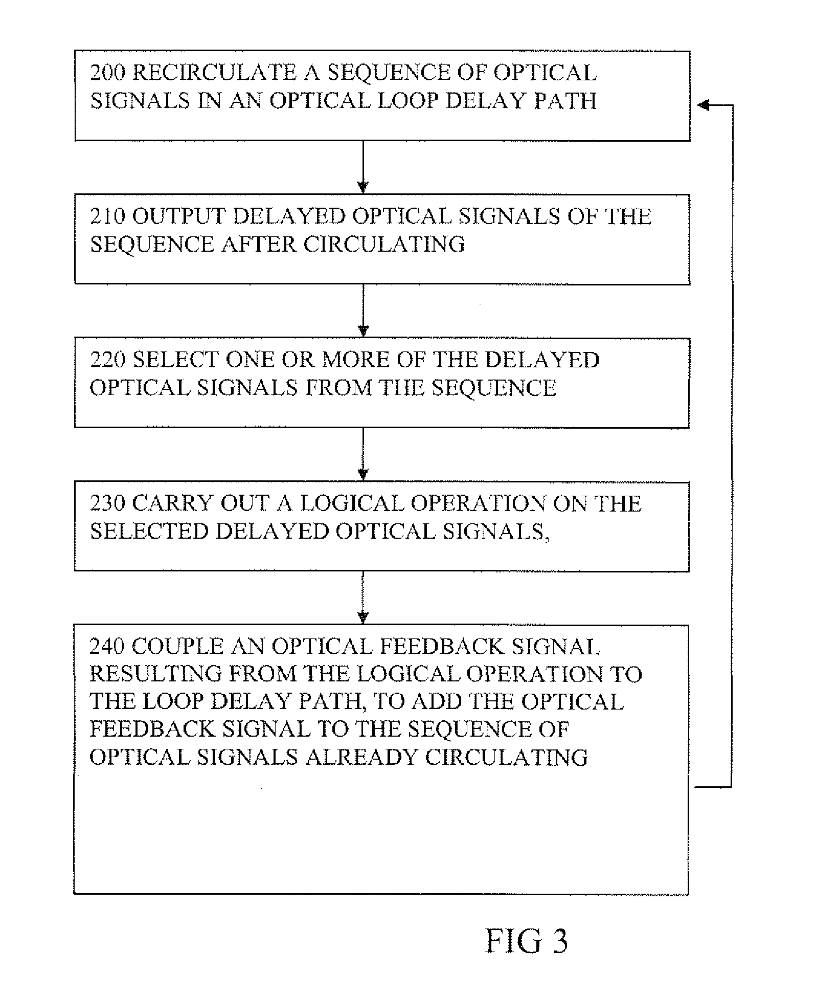
An optical linear feedback circuit has an optical loop delay path (10) for recirculating a sequence of optical signals, and an output path for outputting delayed optical signals after circulating one or more times around the loop. A selector (50) is provided for selecting one or more of the delayed optical signals from the sequence, and an optical logic circuit (20) is coupled to carry out a logical operation on the selected delayed optical signals to create an optical feedback signal which is coupled to the optical loop delay path, so that the optical feedback signal can be added to the sequence of optical signals already circulating. By recirculating around a loop, each round trip can be regarded as equivalent to a shift of a shift register, so longer sequences can be built up without needing an additional storage cell for each shift function.

Description

CROSS REFERENCE TO RELATED APPLICATION[0001]The disclosure of Europe Patent Application No. 11155851.6, filed on Feb. 24, 2011, is incorporated herein by reference.TECHNICAL FIELD[0002]This invention relates to optical linear feedback circuits, to nodes having such circuits, and to corresponding methods of operating such circuits.BACKGROUND[0003]Memory elements are key components of all the electronic central processing units (CPU) as for example shift registers within the arithmetic logic units to perform operations as multiplication and division. CPUs are connected with random access memory (RAM) slots to store and read data to be processed. Telecom applications require memory elements as well. Buffers within the network nodes store information when a contention occurs at an output port. Shift registers are employed for serial to parallel conversion and cyclic operations. Error detection and correction techniques such as parity check, or cyclic redundancy check can be implemented ...

Claims


Application Information

Patent Timeline
Patent Type & Authority Patents(United States)
IPC IPC(8): H04B10/299G02F3/00
CPCG11C21/00G11C13/04G06E1/02G11C19/00
Inventor SCAFFARDI, MIRCOBERRETTINI, GIANLUCABOGONI, ANTONELLA
Owner TELEFON AB LM ERICSSON (PUBL)
Learn More