Semiconductor structure with improved capacitance of bit line

a technology of semiconductors and capacitors, applied in semiconductor devices, semiconductor/solid-state device details, electrical apparatus, etc., can solve the problems of increasing delay in transmitting bit signals, and achieve the effect of avoiding high signal delay, and improving the capacitance of bit lines

Active Publication Date: 2014-04-22
MACRONIX INT CO LTD
View PDF4 Cites 8 Cited by
  • Summary
  • Abstract
  • Description
  • Claims
  • Application Information

AI Technical Summary

Benefits of technology

[0005]The invention is directed to a semiconductor structure with improved capacitance of bit lines. In an embodiment, an independent control circuit is disposed into the 3D stack memory so that the capacitance of each stack block is independent or some capacitances of the stack blocks are connected in parallel. Thus, a signal delay due to high capacitance of bit lines is avoided.

Problems solved by technology

However, in the 3D stack structure, the bit lines connected to different stack blocks make the capacitance of each stack blocks in parallel, and the capacitances of the stack blocks summed up results in an increase of the capacitance of the bit lines, causing a delay for transmitting the bit signals.

Method used


Image

  • Semiconductor structure with improved capacitance of bit line
  • Semiconductor structure with improved capacitance of bit line
  • Semiconductor structure with improved capacitance of bit line

Examples


first embodiment

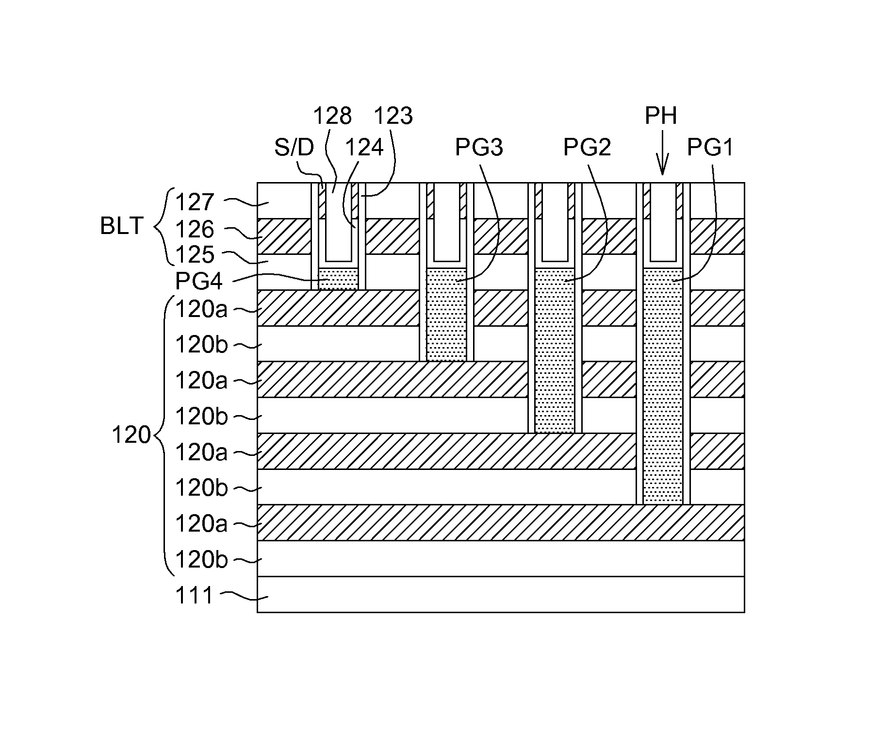
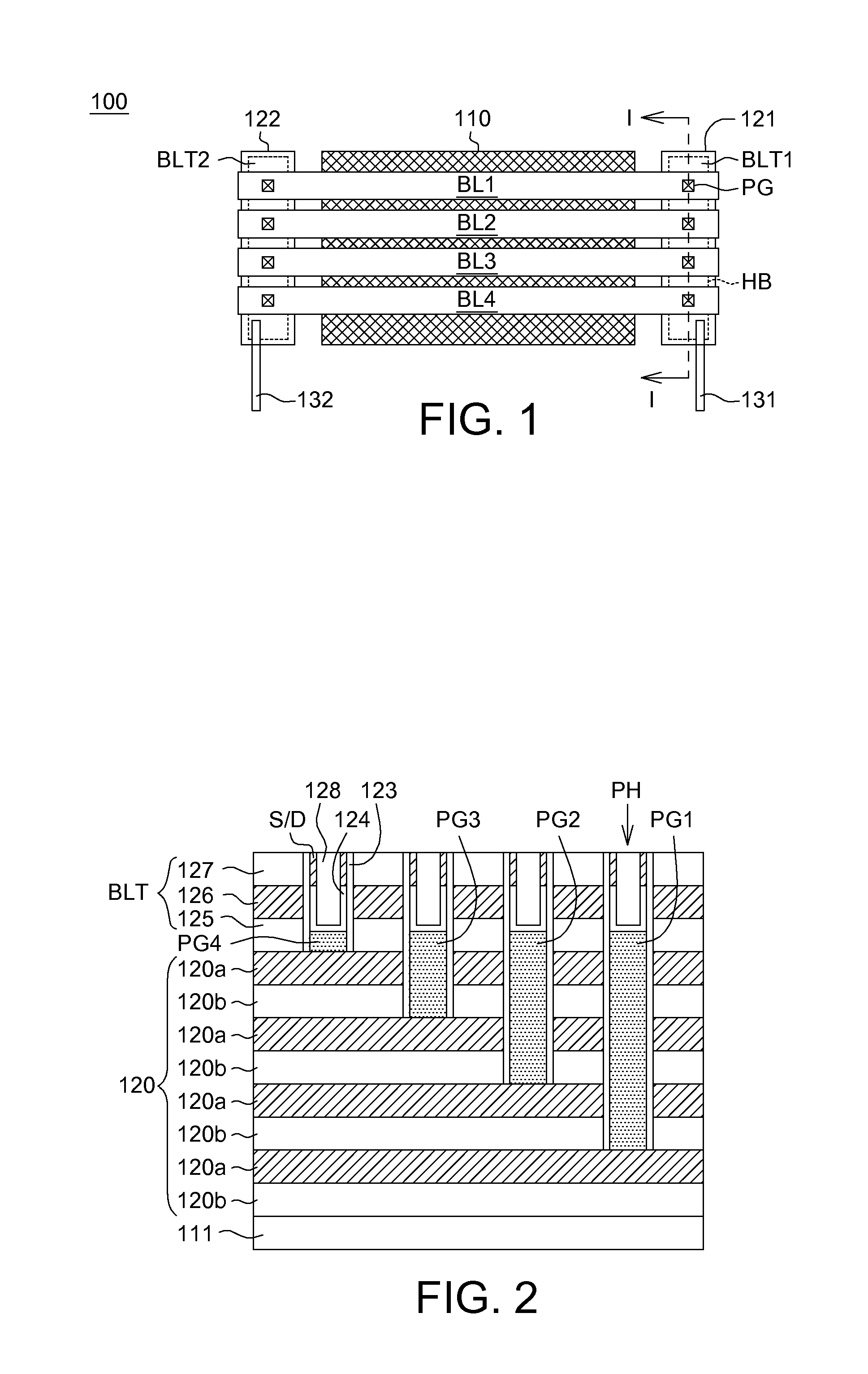
[0021]Referring to FIG. 1, a top schematic view of a semiconductor structure 100 with improved capacitance of bit lines according to an embodiment of the invention is shown. Taken four bit lines BL1-BL4 arranged in order for example, a stacked memory structure 110 is located between a first stair contact structure 121 and a second stair contact structure 122. The stacked memory structure 110, for example 3D NAND flash memory, has multi-layers of memory planes arranged from bottom to top in order. A first bit line BL1 is connected to a first layer of memory plane via the first stair contact structure 121, and a second bit line BL2 is connected to a second layer of memory plane via the first stair contact structure 121, and so on. Similarly, various bit lines BL1-BL4 can be connected to different memory planes via the second stair contact structure 122. In an embodiment, the first stair contact structure 121 and the second stair contact structure 122 are connected to the first conduct...

second embodiment

[0032]Referring to FIG. 7, a top schematic view of a semiconductor structure 101 with improved capacitance of bit lines according to another embodiment of the invention is shown. In the above embodiment, a group of transistor structures BLT is formed on the top of the stair contact structure 120, while a group of transistor structures BLT1′ (BLT2′) formed on a side of the stair contact structure 121 (122′) and a conductive line 131′ (132′) connected to the gate of the group of transistor structures BLT1′ (BLT2′) are disclosed in the present embodiment. The conductive line input a voltage to selectively open or close the transistor structures BLT1′ (BLT2′). The details of description of the bit lines BL1-BL4 (BL1′-BL4′), the first stair contact structure s 121 (121′), the second stair contact structure s 122 (122′) and the stacked memory structure 110 (110′) are similar to the structures disclosed in the first embodiment, and do not repeat again.

[0033]Referring to FIG. 8, the first s...


PUM


Abstract

A semiconductor structure with improved capacitance of bit lines includes a substrate, a stacked memory structure, a plurality of bit lines, a first stair contact structure, a first group of transistor structures and a first conductive line. The first stair contact structure is formed on the substrate and includes conductive planes and insulating planes stacked alternately. The conductive planes are separated from each other by the insulating planes for connecting the bit lines to the stacked memory structure by stairs. The first group of transistor structures is formed in a first bulk area where the bit lines pass through and then connect to the conductive planes. The first group of transistor structures has a first gate around the first bulk area. The first conductive line is connected to the first gate to control the voltage applied to the first gate.

Description

BACKGROUND[0001]1. Technical Field[0002]The invention relates in general to a semiconductor structure, and more particularly to a semiconductor structure with improved capacitance of bit lines.[0003]2. Description of the Related Art[0004]With the development of semiconductor technology, the demand for the memory device focuses on small size and larger memory capacity. For satisfying the requirement, a memory device having a high element density is need. Since the critical dimension of the memory device has been decreased to the ultimate in the art, designers develop a structure for improving the density of memory, using 3D stack memory device so as to increase the memory capacity and lower the size per cell. However, in the 3D stack structure, the bit lines connected to different stack blocks make the capacitance of each stack blocks in parallel, and the capacitances of the stack blocks summed up results in an increase of the capacitance of the bit lines, causing a delay for transmi...

Claims


Application Information

Patent Timeline
Patent Type & Authority Patents(United States)
IPC IPC(8): H01L47/00
CPCH01L47/00H01L27/11556H01L27/11548H01L27/11575H01L27/11582H10B41/50H10B41/27H10B43/50H10B43/27
Inventor CHEN, SHIH-HUNGLUE, HANG-TINGHSIEH, KUANG-YEULAI, ERH-KUNSHIH, YEN-HAO
Owner MACRONIX INT CO LTD
Why Eureka
Try Eureka